• Journal of Semiconductors
  • Vol. 41, Issue 12, 122802 (2020)
Wen Gu1、2, Zhibin Liu1、2、3, Yanan Guo1、2、3, Xiaodong Wang1、2、3, Xiaolong Jia4, Xingfang Liu2、5, Yiping Zeng4、5、6, Junxi Wang1、2、3, Jinmin Li1、2、3, and Jianchang Yan1、2、3
Author Affiliations
  • 1Research and Development Center for Solid-State Lighting, Institute of Semiconductors, Chinese Academy of Sciences, Beijing 100083, China
  • 2Center of Materials Science and Optoelectronics Engineering, University of Chinese Academy of Sciences, Beijing 100049, China
  • 3Beijing Engineering Research Center for the 3rd Generation Semiconductor Materials and Application, Beijing 100083, China
  • 4Advanced Ultraviolet Optoelectronics Co. Ltd, Changzhi 046000, China
  • 5Key Laboratory of Semiconductor Materials Science, Institute of Semiconductors, Chinese Academy of Sciences, Beijing 100083, China
  • 6Youwill Hitech Co. Ltd, Beijing 100083, China
  • show less
    DOI: 10.1088/1674-4926/41/12/122802 Cite this Article
    Wen Gu, Zhibin Liu, Yanan Guo, Xiaodong Wang, Xiaolong Jia, Xingfang Liu, Yiping Zeng, Junxi Wang, Jinmin Li, Jianchang Yan. Comprehensive study of crystalline AlN/sapphire templates after high-temperature annealing with various sputtering conditions[J]. Journal of Semiconductors, 2020, 41(12): 122802 Copy Citation Text show less

    Abstract

    High-quality AlN/sapphire templates were fabricated by the combination of sputtering and high-temperature (HT) annealing. The influence of sputtering parameters including nitrogen flux, radio frequency power, and substrate temperature on the crystalline quality and surface morphology of annealed AlN films were investigated. With lower substrate temperature, lower power, and lower N2 flux, the full width at half maximum of the X-ray rocking curve for AlN (0002) and (10 2) were improved to 97.2 and 259.2 arcsec after high-temperature annealing. This happens because the increased vacancy concentration of sputtered AlN films can facilitate the annihilation of dislocations by increasing the recovery rate during HT annealing. Step and step-bunching morphologies were clearly observed with optimized sputtering conditions.

    1. Introduction

    AlN is of great potential in the implantation of deep ultraviolet (DUV) emitters because of its wide bandgap (~6.2 eV), excellent UV transparency and high thermal conductivity[1, 2]. Low threading dislocation density (TDD) is necessary to improve the quantum efficiency of UV light-emitting diodes (LEDs)[3]. Recently, the bulk AlN substrate with a dislocation density (DD) of 103 cm–2 has been achieved[4, 5]. However, the high impurity concentration and high cost has made it inferior to the AlN/sapphire template for commercial motivations. To date, the reported full width at half maximum (FWHM) values of (0002)- and (10 2)-plane of AlN grown by MOCVD have been reduced to 79 and 206 arcsec[6]. Meanwhile, due to the large lattice and thermal expansion coefficient mismatches between AlN and sapphire, AlN grown on sapphire by metal-organic chemical vapor deposition (MOCVD) system still suffers from the TDD higher than 108 cm–2[7], although many methods have been proposed to reduce the TDD of AlN films grown on sapphire, such as periodical high/middle-temperature AlN growth method[8], ELOG method[9], the nano-patterned sapphire substrates (NPSS)[10], and two-phase growth method[11]. Moreover, the serious pre-reaction of trimethylaluminum (TMAl) and ammonia (NH3)[12], the poor uniformity of temperature distribution in the chamber, and rapid consumption of heater at high temperature (HT) limit the yield of AlN films by MOCVD with small-size reactor and lead to the high cost of UVC LEDs. To improve the productivity and quality of AlN/sapphire template, and reduce the cost of UVC LEDs, a method that combines sputtering and HT annealing technologies outside MOCVD has been reported[13, 14]. For example, the annealing of low temperature AlN buffer layer has shown remarkable improvement of crystalline quality and the FWHM values were 59 and 284 arcsec for the (0002)- and (10 2)-plane[15]. Besides, the FWHM values of (0002)- and (10 2)-plane of annealed sputtered AlN were also reduced to 36 and 260 arcsec, respectively[16]. The effect of annealing temperature and the thickness of AlN films sputtered with AlN targets on the sapphire substrate has been investigated[17]. However, few reports concentrate on the sputtering parameters with Al target during depositing AlN, which has complicated formation mechanisms. In this work, the effects of sputtering parameters, including power, temperature, and N2 flux, on the crystallinity evolution of annealed AlN films are systematically investigated. The correlations between the sputtering process and HT annealing are comprehensively discussed.

    2. Experiment

    In this experiment, AlN layers with a target thickness of 200 nm were deposited on 2-inch c-plane sapphire by radio frequency (RF) reactive magnetron sputtering. High-purity Al (> 99.9999 at%) was used as the target. The RF power was set to 2000 and 3000 W. N2 was used as the sputtering gas in the range of 100–180 sccm, and the substrate temperature was changed from 550 to 700 °C. The chamber background pressure was lower than 3.2 × 10⁻⁵ Pa, and the process pressure was varied from 0.31 to 0.55 Pa as the increase of N2 flux. The deposition rate of the sputtered particles was in the range of 0.20–0.35 nm/s, which is mainly determined by RF power[18]. These parameters and characterizations of sputtered AlN are presented in Tables 1 and 2, respectively. Subsequently, the sputtered AlN was annealed in N2 at 1700 °C for 3 h. During the annealing process, the pressure was kept at the atmosphere and the “face to face” method was applied to suppress AlN decomposition[19]. The crystallinity of sputtered and annealed AlN films was investigated by Bede D1 X-ray diffraction (XRD). The FWHM of (0002)- and (10 2)-plane were adopted to evaluate the tilt and twist components. The surface morphology evolution was determined by Veeco Dimension 3100 atomic force microscopy (AFM). Raman spectroscopy measurement was performed to analyze the stress state.

    Table Infomation Is Not EnableTable Infomation Is Not Enable

    3. Results and discussion

    3.1. The effect of substrate temperature

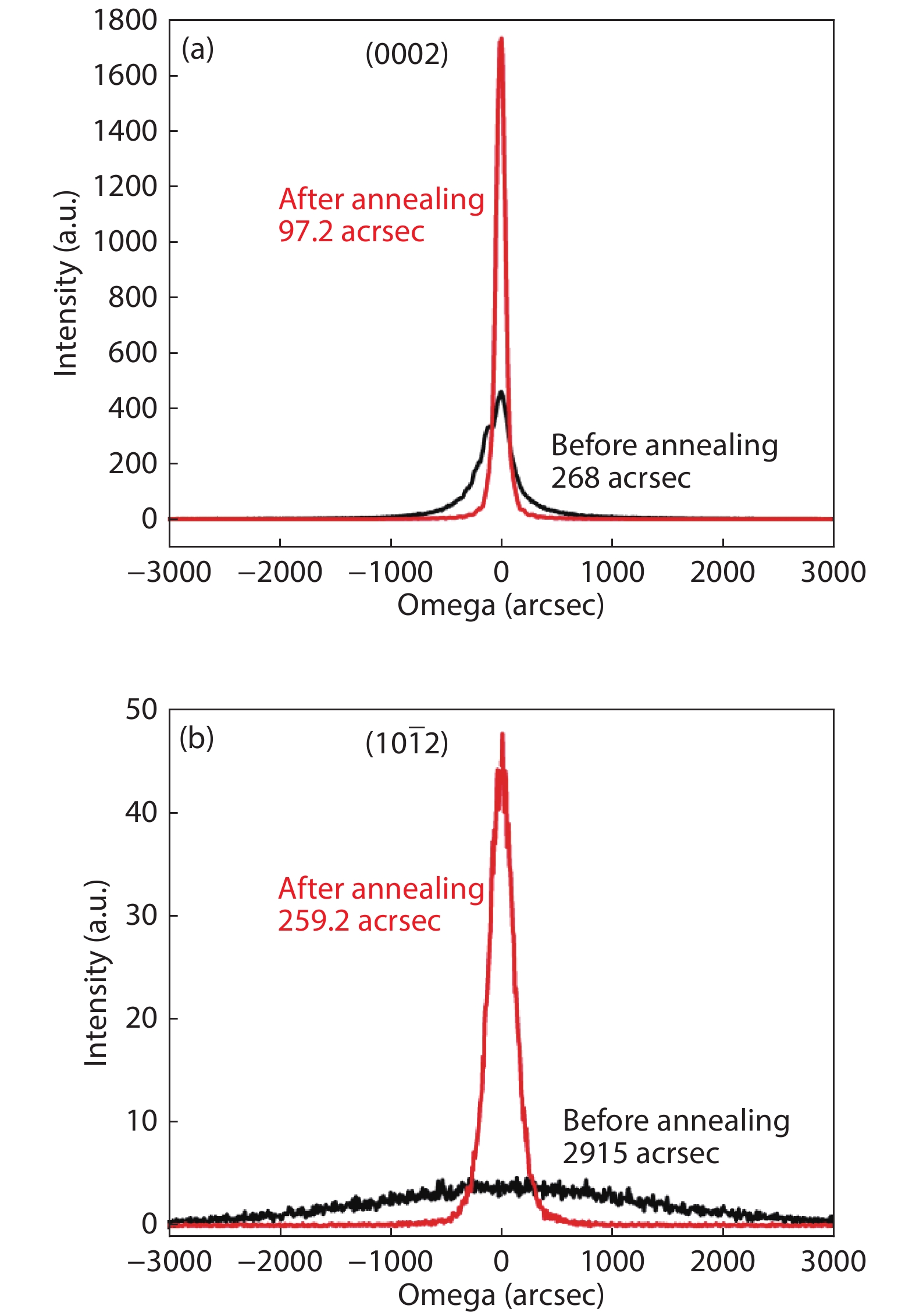
    Fig. 1 shows the (0002)- and (10 2)-plane XRCs of the 200-nm AlN films sputtered at 2000 W and 600 °C with a N2 flux of 100 sccm before and after annealing. Before annealing, the (0002)-plane XRC of sputtered AlN films shows a distinct peak in Fig. 1(a) and the FWHM value is as low as 268 arcsec. A side peak is also observed, which implies the incoherent crystallographic orientation of the sputtered AlN. Due to the low deposition temperature during sputtering, the (10 2)-plane XRC in Fig. 1(b) shows a board peak feature and the FWHM value is 2915 arcsec. These FWHM values indicate that the orientations of sputtered AlN films are composed of low tilt component and high twist component. After HT annealing, the side peak of (0002)-plane disappear. Moreover, the FWHM values of (0002)- and (10 2)-plane are dramatically reduced to 97.2 and 259.2 arcsec. The remarkable crystallinity improvement of AlN films after HT annealing is due to the higher recovery rate or further reduction in the dislocation density, which happens because the high vacancy concentration in sputtered AlN films or a faster diffusion process improves dislocation climb during annealing[20, 21].

    (Color online) The (a) (0002)- and (b) (102)-plane XRCs of the AlN films sputtered at 2000 W, 600 °C and 100 sccm N2 before and after HT annealing.

    Figure 1.(Color online) The (a) (0002)- and (b) (10 2)-plane XRCs of the AlN films sputtered at 2000 W, 600 °C and 100 sccm N2 before and after HT annealing.

    To better comprehend the impact of substrate temperature on the crystallinity of annealed AlN films, AlN films with various substrate temperatures are applied. Fig. 2 shows the effect of substrate temperature on the FWHM values of (10 2)-plane of the annealed AlN films sputtered at 550, 600, 650, 700 °C with a N2 flux of 100 sccm. For the annealed AlN films which are sputtered at 3000 W, the FWHM values of (10 2)-plane are gradually reduced from 367.2 to 313.2, 284.4, 280.8 arcsec as the reduction of substrate temperature. Meanwhile, the FWHM values of (10 2)-plane of the annealed AlN films sputtered at 2000 W are also reduced from 356.4 to 273.6, 259.2 arcsec as the substrate temperature decreases from 700 to 600 °C. However, the FWHM value of (10 2)-plane increases to 280.8 arcsec for the annealed AlN films sputtered at 550 °C and 2000 W. Besides, the FWHM values of (0002)-plane of all the annealed AlN films are reduced to lower than 100 arcsec and are similar (not shown here), indicating the great elimination of the tilt component.

    (Color online) The FWHM values of (102)-plane of the annealed AlN films with different substrate temperatures at 2000 and 3000 W.

    Figure 2.(Color online) The FWHM values of (10 2)-plane of the annealed AlN films with different substrate temperatures at 2000 and 3000 W.

    The relationship between the FWHM values of (10 2)-plane of the annealed AlN and the substrate temperature are studied by the tilt components of sputtered AlN films obtained from the (0002)-plane XRC and Raman measurement. As shown in Fig. 3(a), for the AlN films sputtered at 2000 W, the (0002)-plane XRC of AlN film deposited at 550 °C has two side peaks. It is because that this lower substrate temperature provides insufficient energy for AlN deposition and causes more tilt component[22]. This lower sputter temperature also leads to higher vacancy concentration during sputtering. It is possible that the more tilt component or the too much vacancy prevents the vacancies from diffusion and stop dislocation climb. Thus, the crystallinity of the annealed AlN film sputtered at 2000 W and 550 °C deteriorates. As the substrate temperature increases from 600 to 700 °C, only one side peak exists and tends to disappear and the FWHM value is reduced, which is attributed to the enhanced surface migration of Al atoms as the increase of substrate temperature[23]. As a result, the tilt component of the sputtered AlN shrinks, and the vacancy concentration is reduced. In this case, the reduced vacancy concentration is the key point to prevent dislocation climb. Therefore, the FWHM value of (10 2)-plane of the annealed AlN increases with increasing sputter temperature and has the minimum value of 259.2 arcsec at 600 °C. In the 3000 W case, the FWHM values of (10 2)-plane of the annealed AlN increases with increasing sputter temperature because of less vacancy density. However, with the substrate temperature increases from 550 to 600 °C, the side peak intensity also increases in Fig. 3(b), which means the more tilt component. Further studies are expected to explain this phenomenon.

    (Color online) The (0002)-plane XRCs of the AlN films sputtered at (a) 2000 and (b) 3000 W with various substrate temperatures before HT annealing.

    Figure 3.(Color online) The (0002)-plane XRCs of the AlN films sputtered at (a) 2000 and (b) 3000 W with various substrate temperatures before HT annealing.

    Figs. 4(a) and 4(b) show the Raman spectrum of AlN films sputtered at various temperatures before annealing. The E2(high) peak frequency is presented in Fig. 4(c). The peak intensity of strain-free AlN films was reported at the phonon frequency of 657.4 cm–1[24]. The smaller (larger) peak frequency indicates a larger tensile (compressive) stress. Before annealing, the E2(high) peak frequency of AlN films sputtered at 2000 W is gradually increased from 654.686 to 660.488 cm–1 as the substrate temperature increases. This means that the stress state of sputtered AlN films can be modulated from tensile to compressive stress by increasing the substrate temperature[25]. It is possibly because of the less vacancy density and dislocation density with higher sputter temperature. The 3000 W case has the similar tendency. However, the stress becomes from tensile to compressive at 600 °C because of less vacancy density and less dislocation density than the 2000 W case. After HT annealing, all the E2(high) peak frequencies of AlN films are higher than 657.4 cm–1 and similar, implying all AlN films have compressive stress after annealing due to the lattice and thermal expansion mismatch between sapphire and AlN in the recrystallization process[26].

    (Color online) Raman spectrum of the AlN films sputtered at (a) 2000 and (b) 3000 W, a N2 flux of 100 sccm, and various substrate temperatures before annealing. (c) The E2(high) peak frequency of sputtered and annealed AlN films with different substrate temperatures.

    Figure 4.(Color online) Raman spectrum of the AlN films sputtered at (a) 2000 and (b) 3000 W, a N2 flux of 100 sccm, and various substrate temperatures before annealing. (c) The E2(high) peak frequency of sputtered and annealed AlN films with different substrate temperatures.

    Fig. 5 shows AFM images (5 × 5 μm2) of the AlN films sputtered at 2000 W and a N2 flux of 100 sccm with different substrate temperatures before and after HT annealing. The surface morphologies of the sputtered AlN films show high-density and uniform column structures in Fig. 5(a)[17]. The diameter and altitude of the columns are increased as the substrate temperature increases from 550 to 650 °C (increased size and number of white dots on the surfaces in these images), which is also demonstrated by the enlarged root mean square (RMS) from 0.852 to 2.20 nm. This may happen because the high substrate temperature will promote the deposition rate and increase the grain size of the AlN column[23]. However, as the substrate temperature further increases to 700 °C, the surface morphology is improved with small-size columns and RMS is reduced to 0.988 nm possibly because the reduced deposition rate and the increased nucleation density at the very start of sputtering. The 3000 W case has a similar trend (not shown here). After HT annealing, the column structures coalesce and a few pits (defects marked in the images) are observed, which were also mentioned in previous work[17]. For the annealed AlN films with low substrate temperature in Figs. 5(e) and 5(f), step-bunching morphology is formed after annealing, and sparse high-altitude columns still exist on the surface and decreases with increasing substrate temperature. When the substrate temperature increases to 700 °C, step morphologies with the RMS of 0.275 nm appear free of high-altitude columns in Fig. 6(h). All of the surfaces of samples with 3000 W after HT annealing have step morphologies (not shown here). The significant improvement of surface morphology after HT annealing is attributed to the coalescence of columnar domains and the annihilation of domain boundaries[17].

    (Color online) 5 × 5 μm2 AFM images of the AlN films sputtered at 2000 W, a N2 flux of 100 sccm and substrate temperatures of (a) 550, (b) 600, (c) 650 and (d) 700 °C before annealing and (e) 550, (f) 600, (g) 650 and (h) 700 °C after annealing.

    Figure 5.(Color online) 5 × 5 μm2 AFM images of the AlN films sputtered at 2000 W, a N2 flux of 100 sccm and substrate temperatures of (a) 550, (b) 600, (c) 650 and (d) 700 °C before annealing and (e) 550, (f) 600, (g) 650 and (h) 700 °C after annealing.

    The effect of N2 flux on the FWHM values of (102)-plane of the annealed AlN films.

    Figure 6.The effect of N2 flux on the FWHM values of (10 2)-plane of the annealed AlN films.

    3.2. The effect of N2 flux

    N2 has two functions during the sputtering process, involving that (1) N2 is ionized as N source to bombard the Al target and form AlN and (2) N2 acts as environment gas and collides with sputtered particles. To reveal the effect of N2 flux during the sputtering process on the crystallinity of annealed AlN films, three different N2 fluxes of 100, 150, 180 sccm are used to deposit AlN at 600 °C. Fig. 6 shows the FWHM values of (10 2)-plane for these sputtered AlN films after HT annealing. For the annealed AlN films sputtered at 2000 W, the FWHM values of (10 2)-plane are increased from 259.2 to 342 arcsec as the increase of N2 flux. Meanwhile, in 3000 W case, the FWHM values of (10 2)-plane of the annealed AlN films also increases from 284.4 to 360 arcsec along with the increase of the N2 flux. All the FWHM values of (0002)-plane are reduced to around 97.2 arcsec after annealing.

    To further analyze the crystallinity evolution of annealed AlN films with the increase of N2 flux during sputtering, the tilt component of sputtered AlN films is investigated. Fig. 7 shows the (0002)-plane XRCs of the AlN films sputtered with various N2 fluxes at 600 °C, 2000 W and 3000 W before annealing. For the AlN films sputtered at 2000 W, all samples have side peaks. Furthermore, the normalized intensity of side peaks decrease with decreasing N2 flux, which means the less tilt component. The 3000 W case has a similar tendency. During sputtering, the process pressure is decreased as the decrease of N2 flux. This will result in a longer mean free path of particles, which means that sputtered Al particles from Al target have less possibility to collide with N2 molecules from target to substrate. Thus, less energy of the sputtered Al will be lost in this process and AlN will deposit on the surface with higher energy, which will lead to less tilt component. This lower tilt component will possibly improve the vacancy diffusion. Hence, the FWHM values of (10 2)-plane are reduced as the decrease of N2 flux mainly due to the less tilt component.

    (Color online) The (0002)-plane XRCs of the AlN films sputtered at (a) 2000 and (b) 3000 W before annealing with various N2 fluxes.

    Figure 7.(Color online) The (0002)-plane XRCs of the AlN films sputtered at (a) 2000 and (b) 3000 W before annealing with various N2 fluxes.

    Fig. 8 presents AFM images (5 × 5 μm2) of the sputtered AlN films sputtered at 2000 W, 600 °C with various N2 fluxes before and after HT annealing. Before annealing, the size and altitude of column structures are increased as the increase of N2 flux and the RMS values are increased from 1.51 to 1.93 nm. After HT annealing, step-bunching structures are formed due to the coalescence of column structures. Moreover, high-altitude columns tend to disappear with the increase of N2 flux. However, lots of voids are observed for the annealed AlN films with a N2 flux of 180 sccm, which are ascribed to the remained residual spaces after the coalescence of domains[17].

    (Color online) AFM images of the AlN films sputtered at 2000 W and 600 °C with N2 fluxes of (a) 100, (b) 150 and (c) 180 sccm before annealing and (d) 100, (e) 150 and (f) 180 sccm after annealing.

    Figure 8.(Color online) AFM images of the AlN films sputtered at 2000 W and 600 °C with N2 fluxes of (a) 100, (b) 150 and (c) 180 sccm before annealing and (d) 100, (e) 150 and (f) 180 sccm after annealing.

    3.3. The effect of RF power

    The effect of RF power can be analyzed by comparing the 2000 and 3000 W cases in the previous parts. Fig. 3 and Fig. 7 show that the 3000 W case has narrower (0002)-plane XRC of sputtered AlN films than 2000 W case with the same other sputtering conditions. It is because the higher RF power provides high kinetic energy for AlN during sputtering which lead to less tilt component. However, the FWHM values of (10 2)-plane of annealed 3000 W samples are higher than that of 2000 W samples, as shown in Figs. 3 and 7, possibly because of less vacancy density. In addition, the surface morphology could maintain the step and step-bunching structures.

    By further reducing the RF power to 1000 W, the color of sputtered AlN films will change from transparent to light yellow due to the lower deposition energy (not shown here). The FWHM values of (10 2)-plane of the annealed AlN sputtered at 1000 W become higher than that sputtered at 2000 W because of the more title component (not shown here).

    4. Conclusion

    The effect of sputtering parameters on the annealed AlN films is comprehensively studied. The high-quality annealed AlN films are obtained at lower substrate temperature, lower N2 flux, and lower RF power. The lower substrate temperature and lower RF power provide less energy for AlN deposition during sputtering, which leads to the increased tilt component and high vacancy concentration. A high vacancy will increase dislocation annihilation by improving dislocation climb during HT annealing. However, a vacancy concentration that is too high or too much of a tilt component will prevent the vacancy from diffusion or stop the dislocation climb. The transformation from compressive stress to tensile stress of sputtered AlN films may also be useful for AlN columns to twist. Lower N2 flux reduces the energy loss by decreasing the collision possibility of sputtered Al particles and N2 molecules, and thus improves the tilt component, which will improve vacancy diffusion. Finally, the FWHM of the (0002) and (10 2)-plane of AlN films after annealing are improved to 97.2 and 259.2 arcsec at the substrate temperature of 600 °C, a N2 flux of 100 sccm and a RF power of 2000 W, corresponding to the screw and edge-type TDD of 2.06 × 10⁷ and 7.52 × 108 cm–2, respectively. By modulating these sputtering parameters, step and step-bunching morphologies with a very low RMS are achieved. We expect to further reveal the crystallinity evolution of annealed AlN with various sputtering conditions in the future.

    Acknowledgements

    This work was supported by the National Key R&D Program of China (Nos. 2016YFB0400800 and 2017YFB0404202), the National Natural Sciences Foundation of China (Grant Nos. 61527814, 61674147, 61904176, U1505253), Beijing Nova Program Z181100006218007 and Youth Innovation Promotion Association CAS 2017157.

    References

    [1] J M Li, Z Liu, Z Q Liu et al. Advances and prospects in nitrides based light-emitting-diodes. J Semicond, 37, 061001(2016).

    [2] Z H Wu, J C Yan, Y N Guo et al. Study of the morphology evolution of AlN grown on nano-patterned sapphire substrate. J Semicond, 40, 122803(2019).

    [3] P Dong, J C Yan, Y Zhang et al. AlGaN-based deep ultraviolet light-emitting diodes grown on nano-patterned sapphire substrates with significant improvement in internal quantum efficiency. J Cryst Growth, 395, 9(2014).

    [4] D Ehrentraut, Z Sitar. Advances in bulk crystal growth of AlN and GaN. MRS Bull, 34, 259(2009).

    [5] R Dalmau, B Moody, R Schlesser et al. Growth and characterization of AlN and AlGaN epitaxial films on AlN single crystal substrates. J Electrochem Soc, 158, H530(2011).

    [6] F J Xu, L S Zhang, N Xie et al. Realization of low dislocation density AlN on a small-coalescence-area nano-patterned sapphire substrate. CrystEngComm, 21, 2490(2019).

    [7] J C Yan, J X Wang, N X Liu et al. High quality AlGaN grown on a high temperature AIN template by MOCVD. J Semicond, 30, 103001(2009).

    [8] J C Yan, J X Wang, Y Zhang et al. AlGaN-based deep-ultraviolet light-emitting diodes grown on High-quality AlN template using MOVPE. J Cryst Growth, 414, 254(2015).

    [9] X Chen, Y Zhang, J C Yan et al. Deep-ultraviolet stimulated emission from AlGaN/AlN multiple-quantum-wells on nano-patterned AlN/sapphire templates with reduced threshold power density. J Alloy Compd, 723, 192(2017).

    [10] P Dong, J C Yan, J X Wang et al. 282-nm AlGaN-based deep ultraviolet light-emitting diodes with improved performance on nano-patterned sapphire substrates. Appl Phys Lett, 102, 241113(2013).

    [11] X Chen, J C Yan, Y Zhang et al. Improved crystalline quality of AlN by epitaxial lateral overgrowth using two-phase growth method for deep-ultraviolet stimulated emission. IEEE Photonics J, 8, 1(2016).

    [12] Z J Du, R F Duan, T B Wei et al. Producing deep UV-LEDs in high-yield MOVPE by improving AlN crystal quality with sputtered AlN nucleation layer. J Semicond, 38, 113003(2017).

    [13] C Huang, P Wu, K Chang et al. High-quality and highly-transparent AlN template on annealed sputter-deposited AlN buffer layer for deep ultra-violet light-emitting diodes. AIP Adv, 7, 055110(2017).

    [14] N Susilo, S Hagedorn, D Jaeger et al. AlGaN-based deep UV LEDs grown on sputtered and high temperature annealed AlN/sapphire. Appl Phys Lett, 112, 041110(2018).

    [15] M X Wang, F J Xu, N Xie et al. Crystal quality evolution of AlN films via high-temperature annealing under ambient N2 conditions. CrystEngComm, 20, 6613(2018).

    [16] S Tanaka, K Shojiki, K Uesugi et al. Quantitative evaluation of strain relaxation in annealed sputter-deposited AlN film. J Cryst Growth, 512, 16(2019).

    [17] S Y Xiao, R Suzuki, H Miyake et al. Improvement mechanism of sputtered AlN films by high-temperature annealing. J Cryst Growth, 502, 41(2018).

    [18] T Kumada, M Ohtsuka, K Takada et al. Influence of sputter power and N2 gas flow ratio on crystalline quality of AlN layers deposited at 823 K by RF reactive sputtering. Phys Status Solidi C, 9, 515(2012).

    [19] H Miyake, C H Lin, K Tokoro et al. Preparation of high-quality AlN on sapphire by high-temperature face-to-face annealing. J Cryst Growth, 456, 155(2016).

    [20] H Fukuyama, H Miyake, G Nishio et al. Impact of high-temperature annealing of AlN layer on sapphire and its thermodynamic principle. Jpn J Appl Phys, 55, 05FL02(2016).

    [21] S Washiyama, Y Guan, S Mita et al. Recovery kinetics in high temperature annealed AlN heteroepitaxial films. J Appl Phys, 127, 115301(2020).

    [22] T Kumada, M Ohtsuka, H Fukuyama. Influence of substrate temperature on the crystalline quality of AlN layers deposited by RF reactive magnetron sputtering. AIP Adv, 5, 017136(2015).

    [23] F Medjani, R Sanjinés, G Allidi et al. Effect of substrate temperature and bias voltage on the crystallite orientation in RF magnetron sputtered AlN thin films. Thin Solid Films, 515, 260(2006).

    [24] S B Yang, R Miyagawa, H Miyake et al. Raman scattering spectroscopy of residual stresses in epitaxial AlN films. Appl Phys Express, 4, 031001(2011).

    [25] Q X Guo, K Yahata, T Tanaka et al. Low-temperature growth of aluminum nitride on sapphire substrates. J Cryst Growth, 257, 123(2003).

    [26] L Zhao, K Yang, Y J Ai et al. Crystal quality improvement of sputtered AlN film on sapphire substrate by high-temperature annealing. J Mater Sci: Mater Electron, 29, 13766(2018).

    Wen Gu, Zhibin Liu, Yanan Guo, Xiaodong Wang, Xiaolong Jia, Xingfang Liu, Yiping Zeng, Junxi Wang, Jinmin Li, Jianchang Yan. Comprehensive study of crystalline AlN/sapphire templates after high-temperature annealing with various sputtering conditions[J]. Journal of Semiconductors, 2020, 41(12): 122802
    Download Citation