
Zheng ZHANG, Yan-Hua ZHANG, Dong-Yue JIN, Wei-Cong NA, Hong-Yun XIE. RF power performance improvement of multi-finger power bipolar transistor by non-uniform emitter finger spacing design without the use of emitter ballasting resistor[J]. Journal of Infrared and Millimeter Waves, 2021, 40(3): 329
- Journal of Infrared and Millimeter Waves
- Vol. 40, Issue 3, 329 (2021)
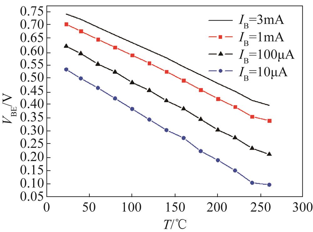
Fig. 1. The measured emitter-base junction voltage VBE as a function of T under different emitter currents of 3 mA, 1 mA, 100 µA and 10 µA respectively
![The schematic diagram of an N-finger HBT, where REi is the emitter ballasting resistor of the ith emitter finger[8-9]](/richHtml/hwyhmb/2021/40/3/329/img_2.jpg)
Fig. 2. The schematic diagram of an N-finger HBT, where REi is the emitter ballasting resistor of the ith emitter finger[8-9]
Fig. 3. The schematic-cross section of a cell in multi-finger HBTs
Fig. 4. Micrographs of the fabricated multi-fingers SiGe HBTs with emitter ballasting resistor.(Note: polysilicon emitter ballasting resistors locate at root terminal of each emitter finger, see the enlarged image)
Fig. 5. Micrograph of the fabricated multi-fingers SiGe HBTs with non-uniform finger spacing
Fig. 6. Measured surface temperature distribution by US QFI Infrared TMS for (a) a multi-finger power HBT with emitter ballasting resistor, and (b)for a multi-finger power HBT with non-uniform finger spacing under IC=800 mA, VCE=5 V and case temperature of TC=80 ℃
Fig. 7. The block diagram of RF power measurement system
Fig. 8. RF Output power poutversus RF input power pin for two types of multi-fingers power HBTs with emitter ballasting resistor and with non-uniform emitter finger spacing respectively
Fig. 9. Collector efficiency ηCversus RF input power pin for two types of multi-fingers power HBTs with emitter ballasting resistor and with non-uniform emitter finger spacing respectively.
Fig. 10. Power-added-efficiency(PAE) versus RF input power pin for two types of multi-fingers power HBTs with emitter ballasting resistor and with non-uniform emitter finger spacing respectively
|
Table 1. The material parameters of various layers for SiGe HBTs.

Set citation alerts for the article
Please enter your email address
© Copyright 2018-2021 | Chinese Laser Press. All Rights Reserved 沪ICP备15018463号-20