• Journal of Infrared and Millimeter Waves
  • Vol. 40, Issue 3, 329 (2021)
Zheng ZHANG, Yan-Hua ZHANG*, Dong-Yue JIN, Wei-Cong NA, and Hong-Yun XIE
Author Affiliations
  • Faculty of Information Technology, Beijing University of Technology, Beijing 100124, China
  • show less
    DOI: 10.11972/j.issn.1001-9014.2021.03.008 Cite this Article
    Zheng ZHANG, Yan-Hua ZHANG, Dong-Yue JIN, Wei-Cong NA, Hong-Yun XIE. RF power performance improvement of multi-finger power bipolar transistor by non-uniform emitter finger spacing design without the use of emitter ballasting resistor[J]. Journal of Infrared and Millimeter Waves, 2021, 40(3): 329 Copy Citation Text show less

    Abstract

    In this paper, the RF power performance and surface temperature distributions for a multi-finger power hetero-junction bipolar transistor (HBT) with non-uniform emitter finger spacing (NUEFS) without the use of emitter-ballasting-resistor (EBR) are measured, and are compared with a multi-finger power HBT with EBR. The experiment results show that for the multi-finger power HBT with NUEFS, the highest surface temperature is lowered, the uniformity of surface temperature distributions measured by US QFI Infrared TMS is improved, the RF power gain and power-added-efficiency (PAE) are increased compared with the multi-finger power HBT with EBR respectively. These results could be attributed to the improvement in positive thermoelectric feedback and thermal coupling effects among the fingers, and the riddance of adverse impact from emitter-ballasting-resistor used in traditional power HBT.

    Introduction

    Power bipolar junction transistor(BJT) and hetero-junction bipolar transistor(HBT) usually employ multiple emitter fingers in parallel to improve the current handling capability, thermal dissipation capability and RF power performance1-4. However, the self-heating effects(SHE) caused by the power dissipation in every emitter finger and thermal coupling effects(TCE) among emitter fingers result in the increase of temperature of HBTs and non-uniformity of temperature distributions among emitter fingers, and as a consequence, the thermal stability, reliability and RF power performance will degrade significantly4-8. It is obvious that the entire device will fail if any single emitter finger fails. Particularly, the temperatures at the center fingers are hotter than outer fingers. Therefore it will draw much current due to the nature of the positive temperature coefficient of emitter current. Hence additional joule heating is generated, the mechanism is thus regenerative and it ultimately destroys the device. To inhibit positive thermoelectric feedback between emitter current and temperature, and to improve thermal stability and increase current handling capability, the common method is to add a ballasting-resistor RE at emitter so as to compensate for the variation of emitter-base junction voltage VBE by using voltage drop across RE7-12. For examples, Schuppen A. et al.10designed 10 fingers and 60 fingers power HBTs with uniform finger spacing, in which the RE of 6 Ω is added at each emitter to improve thermal effects, the output power was 1W; Potyraj, P. A. et al.11reported multi-finger power HBTs with uniform emitter finger spacing, the TiW ballasting-resistor RE was added at each emitter to improve current handling capability; Ma Z. et al.12 investigated the effects of RE, base-ballasting-resistor RB, and non-ballasting-resistor on the thermal stability of three kinds of 160 fingers HBTs with uniform finger spacing, the results showed that three types of HBTs were all thermally stable under VCE =3 V, the two types of HBTs with RB and RE were thermally stable under VCE =4 V, but only the HBTs with RE was thermally stable under VCE =5 V, and therefore the RE was proved to be more effective in thermal stability improvement compared with RB technique. However, the additional RE at emitter will degrade HBT RF power performance, such as power gain(Gp) and power-added-efficiency(PAE)8-12 no matter how to optimize the RE. As an alternative method, a non-uniform finger spacing technique with large finger spacing in center fingers and small finger spacing in outer fingers for multi-finger HBTs can alleviate thermal coupling effects(TCE) among emitter fingers due to the improvements in thermal flow distribution. Our previous works 13-15 revealed that the non-uniform emitter finger spacing(NUEFS) technique is effective in lowering peak temperature and enhancing uniformity of the temperature profile among emitter fingers compared with uniform emitter finger spacing technique. As an extension of our previous works, in this paper, a comparative study between two types of multi-finger power HBTs with NUEFS and emitter ballasting-resistor(RE) is performed to exhibit the superiority of NUEFS technique in improvements of RF power gain, power-added-efficiency PAE), and temperature profile over emitter ballasting-resistor(RE) technique. To the best of the authors’ knowledge, the comparative study on RF power performances of the two types of multi-finger HBTs is not available in the literature. The paper is arranged as follows. In Section I, the mechanism and disadvantages of the introduction of RE to improve HBT current handling capability are briefly analyzed; the structure and layouts of two types of multi-finger power HBTs with NUEFS and RE are shown in Section II; the measurement results of surface temperature distributions by US QFI Infrared TMS, RF power gain(Gp), collector efficiency(ηC) and power-added-efficiency(PAE) are demonstrated in Section III; the conclusions are given in Section IV.

    1 Mechanism and disadvantages of the introduction of emitter ballasting resistor to improve HBT current handling capability

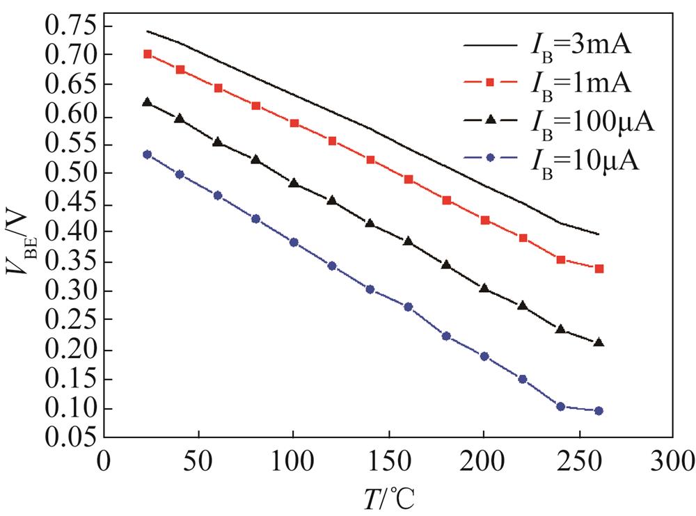
    For an HBT, emitter-base junction voltage VBE varies with temperature T. Figure 1 shows the measured VBE as a function of T under different emitter currents of 3 mA, 1 mA, 100 µA and 10 µA respectively for our a SiGe HBT. The temperature coefficient(dVBE/dT) of VBE can be obtained as -1.53 mV/℃, -1.59 mV/℃, -1.76 mV/℃ and -1.92 mV/℃, respectively. The dVBE/dT is a negative value. Therefore, for an HBT, as the current increases, the temperature increases due to SHE and TCE. As a result, interior VBE decreases. Under external bias keep unchanged, the emitter current will increase, which will further increase dissipation power and lead to temperature rise. Ultimately, the device will be burned out if the measures to restrict the increase of current is not taken.

    The measured emitter-base junction voltage VBE as a function of T under different emitter currents of 3 mA, 1 mA, 100 µA and 10 µA respectively

    Figure 1.The measured emitter-base junction voltage VBE as a function of T under different emitter currents of 3 mA, 1 mA, 100 µA and 10 µA respectively

    In order to alleviate positive thermoelectric feedback between emitter current and temperature, and protect the HBT from thermal burn-out, it is common to add a ballasting-resistor REi at emitter as shown in Fig. 2 so as to compensate the variation of emitter-base junction voltage VBE by using voltage drop across REi.

    The schematic diagram of an N-finger HBT, where REi is the emitter ballasting resistor of the ith emitter finger[8-9]

    Figure 2.The schematic diagram of an N-finger HBT, where REi is the emitter ballasting resistor of the ith emitter finger8-9

    To guarantee thermal stability of HBT within a certain limit of emitter current(IE), the engineering regulation for ballasting resistor RE is as follows: when emitter-base junction temperature varies by ±5 K, the added RE at emitter finger could able to restrict the variation of IE within ±5%, so the minimum emitter ballasting-resistor REmin can be expressed as8-9

    REmin=ΔVΔI=5×(dVBE/dT)0.05×IE=100dVBE/dTIE

    where units of dVBE/dT and IE are mV/℃ and mA respectively.

    We can see that REmin is determined by threshold emitter current(IE), it is only effective for an HBT to thermally stable operate under a certain of emitter current(IE).

    However, on the other hand, the additional emitter ballasting-resistor RE will degrade RF power performance no matter how to optimize the RE. The parameters of power gain(Gp) and power-added-efficiency(PAE), which are employed to characterize RF power performance, are related to ballasting-resistor RE as follows:

    Gp=poutpin=fT8πf2(rb+RE)CTC
    PAE=pout-pinpDC=(1-1Gp)poutpDC=(1-1Gp)ηC

    where pout is RF output power, pin is RF input power, fT is transit frequency, rb is base resistance, CTC is collector output capacitance, PDC is DC power, ηC=pout/PDC is collector efficiency.

    Therefore, Gp and PAE are degraded due to the existence of RE. Furthermore, in order to guarantee the thermal stability of HBT within a certain of emitter current(IE) and power, it is usually suggested that RE >REmin, this could further degrade Gp and PAE.

    2 Structure and layouts of multi-finger power HBTs

    The schematic cross section of a cell of multi-finger HBTs based on SiGe process and the material parameters of various layers of the device are shown in Fig. 3 and Table 1, respectively. The power HBTs is fabricated in Institute of Microelectronics, Tsinghua University.

    The schematic-cross section of a cell in multi-finger HBTs

    Figure 3.The schematic-cross section of a cell in multi-finger HBTs

    compositionThickness/nmDoping concentration/cm-3
    EmitterSi121×1018
    BaseSi0.84Ge0.16302×1019
    CollectorSi4.4×1031×1016
    SubstrateSi1.5×1051×1019

    Table 1. The material parameters of various layers for SiGe HBTs.

    Fig. 4 and Fig. 5 are the micrographs of the fabricated multi-finger power SiGe HBTs with polysilicon as emitter ballasting resistor and non-uniform finger spacing, respectively.

    Micrographs of the fabricated multi-fingers SiGe HBTs with emitter ballasting resistor.(Note: polysilicon emitter ballasting resistors locate at root terminal of each emitter finger, see the enlarged image)

    Figure 4.Micrographs of the fabricated multi-fingers SiGe HBTs with emitter ballasting resistor.(Note: polysilicon emitter ballasting resistors locate at root terminal of each emitter finger, see the enlarged image)

    Micrograph of the fabricated multi-fingers SiGe HBTs with non-uniform finger spacing

    Figure 5.Micrograph of the fabricated multi-fingers SiGe HBTs with non-uniform finger spacing

    3 Measurement results and discussion

    In this section, the measured surface temperature distributions by US QFI Infrared TMS, and the measured power gain(Gp), collector efficiency(ηC) and power-added-efficiency(PAE) for two types of multi-fingers SiGe HBTs with non-uniform finger spacing(NUEFS) and emitter ballasting resistor(EBR) respectively are shown and compared.

    3.1 Surface temperature distributions measurements of multi-fingers power HBTs

    The surface temperature distributions measured by temperature measurement microscope systems(TMS) from US quantum focus instruments(QFI) Corporation for two types of multi-fingers HBTs with emitter ballasting resistor(EBR) and with non-uniform emitter finger spacing(NUEFS) under IC=800 mA, VCE=5 V and case temperature of TC=80℃ are shown in Fig. 6. We can see that the highest temperature is lowered and the maximum temperature difference is improved for the HBTs with NUEFS compared with the HBTs with EBR. Therefore, the temperature distribution uniformity is improved as expected. These results could be attributed to the decrease of the heat flow from adjacent fingers to the center fingers by increasing the spacing between fingers in center region where the thermal-coupling effects are strongest and the alleviation of non-uniform variation of VBE with temperature T.

    Measured surface temperature distribution by US QFI Infrared TMS for (a) a multi-finger power HBT with emitter ballasting resistor, and (b)for a multi-finger power HBT with non-uniform finger spacing under IC=800 mA, VCE=5 V and case temperature of TC=80 ℃

    Figure 6.Measured surface temperature distribution by US QFI Infrared TMS for (a) a multi-finger power HBT with emitter ballasting resistor, and (b)for a multi-finger power HBT with non-uniform finger spacing under IC=800 mA, VCE=5 V and case temperature of TC=80 ℃

    3.2 RF power performance measurements

    The package and RF power measurements of two types of multi-finger power HBTs with non-uniform finger spacing(NUEFS) and emitter ballasting resistor(EBR) are performed by The 13th Research Institute of China Electronic Technology Corporation. The measurement system mainly consists of a power signal source, isolator, directional coupler, test fixture, attenuator, power meter, bias power supply, and so on, as shown in Fig 7.

    The block diagram of RF power measurement system

    Figure 7.The block diagram of RF power measurement system

    The measured output power(poutversus input power(pin), collector efficiency(ηCversus input power(pin), and power-added-efficiency(PAE) versus input power(pin) for two types of multi-fingers SiGe HBTs with emitter ballasting resistor(EBR) and non-uniform emitter finger spacing(NUEFS) under class C operation and at the frequency of 1.2 GHz are shown in Figs.8~10, respectively.

    RF Output power poutversus RF input power pin for two types of multi-fingers power HBTs with emitter ballasting resistor and with non-uniform emitter finger spacing respectively

    Figure 8.RF Output power poutversus RF input power pin for two types of multi-fingers power HBTs with emitter ballasting resistor and with non-uniform emitter finger spacing respectively

    Collector efficiency ηCversus RF input power pin for two types of multi-fingers power HBTs with emitter ballasting resistor and with non-uniform emitter finger spacing respectively.

    Figure 9.Collector efficiency ηCversus RF input power pin for two types of multi-fingers power HBTs with emitter ballasting resistor and with non-uniform emitter finger spacing respectively.

    Power-added-efficiency(PAE) versus RF input power pin for two types of multi-fingers power HBTs with emitter ballasting resistor and with non-uniform emitter finger spacing respectively

    Figure 10.Power-added-efficiency(PAE) versus RF input power pin for two types of multi-fingers power HBTs with emitter ballasting resistor and with non-uniform emitter finger spacing respectively

    As shown, for the multi-fingers SiGe HBTs with EBR, pout increases with the increase of pin, but pout tends to saturate. At pin=0.9 W, the pout=1.9 W, power gain Gp=3.25dB, ηC=72%, and PAE=40%. For the multi-fingers SiGe HBTs with NUEFS, pout increases linearly with the increase of pin and does not saturate. At pin=0.9 W, the pout=4W, power gain Gp=6.48dB, ηC=63%, and PAE=49%. The comparison between the HBT with NUEFS and the HBT with EBR indicates that the pout is increased by 2.1W. This is because that for the same RF input voltage signal, there is not voltage drop across RE in the HBT with NUEFS. Therefore, the current gain is improved, and the collector current ic is increased 16. As a result, the pout is increased according to the expression pout=ic2×RL, where RL is output load impedance. Furthermore, Gp is increased by 3.23 dB, ηC is decreased by 9%, and PAE is increased by 9%. As expected the RF power performance is improved.

    4 Summary and conclusions

    A comparative study of two types of multi-finger power HBTs with non-uniform emitter finger spacing(NUEFS) and emitter-ballasting-resistor(EBR) is performed experimentally in terms of surface temperature distributions, RF power gain and power-added-efficiency(PAE). The experiment results show that for the multi-finger power HBT with NUEFS, not only the uniformity of surface temperature distributions measured by US QFI Infrared TMS but also RF power gain and power-added-efficiency(PAE) is improved compared with a multi-finger power HBT with EBR. These results could be attributed to improvement in positive thermoelectric feedback and thermal coupling effects among the fingers, and the riddance of adverse impact from emitter-ballasting-resistor used in traditional power HBTs.

    References

    [1] Zhi JIN, Wei CHENG, Xin-Yu LIU et al. High current, multi-finger InGaAs/InP hetero-structure bipolar transistor with ft of 176GHz. J. Infrared Millim.Waves, 28, 60-64(2009).

    [2] Ao ZHANG, Yi-Xin ZHANG, Bo-Ran WANG et al. An approach to determine small-signal model parameters for InP HBT up to 110 GHz. J. Infrared Millim.Waves, 37, 688-692(2018).

    [3] Wei CHENG, You-Tao ZHANG, Yuan WANG et al. 0.5μm InP DHBT technology for 100 GHz+ mixed signal integrated circuits. J. Infrared Millim.Waves, 36, 167-172(2017).

    [4] Y H Tu, H C Tseng. Alleviation of thermal Instability via novel collector-up HBTs for reliable wireless applications. IEEE Trans. Dev. Mater. Reliab., 19, 189-192(2019).

    [5] L L Spina, V d’Alessandro, S Russo et al. Influence of concurrent electro-thermal and avalanche effects on the safe operating area of multi-finger bipolar transistors. IEEE Trans. Electron. Dev., 56, 483-491(2009).

    [6] J J Liou, L L Liou, C I Huang. Analytical model for AlGaAs/GaAs multiemitter finger HBT including self-heating and thermal coupling effects. IEEE Proc. Circuits Dev. Syst, 141, 469-476(1994).

    [7] G B Gao, M Z Wang, X Gui et al. Thermal design studies of high-power heterojunction bipolar transistors. IEEE Trans. Electron. Dev., 36, 854-863(1989).

    [8] G B Gao, M S Unlu, H Morkoc et al. Emitter ballasting resistor design for, and AlGaAs/GaAs power heterojunction bipolar transistors. IEEE Trans. Electron. Dev., 38, 185-196(1991).

    [9] R P Arnold, D S Zoroglu. A quantitative study of emitter ballasting. IEEE Trans. Electron. Dev, 21, 385-391(1974).

    [10] A Schuppen, S Gerlach, H Dietrich. 1-W SiGe power HBTs for mobile communication. IEEE Microw. Guided Wave Lett., 6, 341-343(1996).

    [11] P A Potyraj, K J Petrosky, K D Hobart. A 230-watt S-band SiGe heterojunction bipolar transistor. IEEE Trans.Microw.Theory Tech., 44, 2392-2397(1996).

    [12] N Jiang, Z Ma, G Wang. 3-W SiGe power HBTs for wireless applications. Mater. Sci. in Semicond. Processing, 8, 323-326(2005).

    [13] Dong-Yue Jin, Wan-Rong Zhang, Pei Shen et al. Multi-finger power SiGe HBTs for thermal stability enhancement over a wide biasing range. Solid-State Electron, 52, 937-940(2008).

    [14] D Y Jin, W R Zhang, P Shen et al. Structure optimization of multi-finger power SiGe HBTs for thermal stability improvement. Microelectron. Reliab, 49, 382-386(2009).

    [15] R Chen, D Y Jin, W R Zhang et al. Thermal resistance matrix representation of thermal effects and thermal design of microwave power HBTs with two-dimensional array layout. Chin. Phys. B, 28, 098502:1-098502:5(2019).

    [16] J J Gao. Heterojunction bipolar transistor for circuit design—microwave modeling and parameter extraction, 207-243(2015).

    Zheng ZHANG, Yan-Hua ZHANG, Dong-Yue JIN, Wei-Cong NA, Hong-Yun XIE. RF power performance improvement of multi-finger power bipolar transistor by non-uniform emitter finger spacing design without the use of emitter ballasting resistor[J]. Journal of Infrared and Millimeter Waves, 2021, 40(3): 329
    Download Citation