• Journal of Semiconductors
  • Vol. 43, Issue 4, 041102 (2022)
Yong Zhang1 and David J. Smith2
Author Affiliations
  • 1Electrical and Computer Engineering Department, University of North Carolina at Charlotte, Charlotte, NC 28223, USA
  • 2Department of Physics, Arizona State University, Tempe, Arizona 85287, USA
  • show less
    DOI: 10.1088/1674-4926/43/4/041102 Cite this Article
    Yong Zhang, David J. Smith. Comprehensive,in operando, and correlative investigation of defects and their impact on device performance[J]. Journal of Semiconductors, 2022, 43(4): 041102 Copy Citation Text show less
    (Color online) The parallel mode of defect characterization – wafer is cut into pieces for separate studies. Examples used are only for demonstration purposes. They are not necessarily obtained from the same wafer.
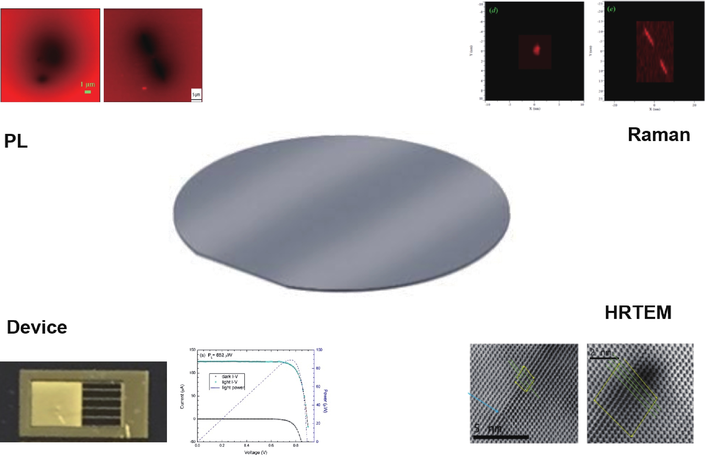
    Fig. 1. (Color online) The parallel mode of defect characterization – wafer is cut into pieces for separate studies. Examples used are only for demonstration purposes. They are not necessarily obtained from the same wafer.
    (Color online) Series mode of defect study. Examples used are only for demonstration purposes. They are not necessarily obtained from the same device.
    Fig. 2. (Color online) Series mode of defect study. Examples used are only for demonstration purposes. They are not necessarily obtained from the same device.
    (Color online) Correlative optical characterization of dislocation defects in a GaAs solar cell. (a) EL image using a 50×/NA0.5 LWD lens for device #5-2, showing a cluster of defects. (b) Optical image of the same area of (a) where red dots indicate defect locations. (c) PL mapping near the defect cluster using a 100×/NA0.9 lens with beam size approximately shown by the size of the red dot in (b). (d) PL spectra from typical defect-free location and the largest defect (#5-2A). (e) Raman mapping near the largest defect (#5-2A). (f) Raman spectra from a typical defect-free location and the largest defect in (e). (reproduced with permission[20])
    Fig. 3. (Color online) Correlative optical characterization of dislocation defects in a GaAs solar cell. (a) EL image using a 50×/NA0.5 LWD lens for device #5-2, showing a cluster of defects. (b) Optical image of the same area of (a) where red dots indicate defect locations. (c) PL mapping near the defect cluster using a 100×/NA0.9 lens with beam size approximately shown by the size of the red dot in (b). (d) PL spectra from typical defect-free location and the largest defect (#5-2A). (e) Raman mapping near the largest defect (#5-2A). (f) Raman spectra from a typical defect-free location and the largest defect in (e). (reproduced with permission[20])
    (Color online) Impact of a defect on solar cell characteristic: left axes forI–V curves (discrete points are experimental data, black solid curves are fitting results), right axes for P–V curves (calculated from experimental data). (a) Cell #5 illuminated under approximate one sun. (b–d) Comparison between a defect-free site and defect site #5-2A, illuminated with a 532 nm focused laser beam under three different laser powers. (reproduced with permission[20])
    Fig. 4. (Color online) Impact of a defect on solar cell characteristic: left axes forI–V curves (discrete points are experimental data, black solid curves are fitting results), right axes for P–V curves (calculated from experimental data). (a) Cell #5 illuminated under approximate one sun. (b–d) Comparison between a defect-free site and defect site #5-2A, illuminated with a 532 nm focused laser beam under three different laser powers. (reproduced with permission[20])
    (Color online) Comparison of different defects. (a, b) PL and Raman mapping of defect #5-2B and #5-2C. (c, d) PL and Raman mapping of defect #5-3A. (e, f) PL and Raman spectra of defect #5-2A-C and #5-3A, and a defect-free site. (g, h) The same in I–V characteristic under two illumination powers. (reproduced with permission[20])
    Fig. 5. (Color online) Comparison of different defects. (a, b) PL and Raman mapping of defect #5-2B and #5-2C. (c, d) PL and Raman mapping of defect #5-3A. (e, f) PL and Raman spectra of defect #5-2A-C and #5-3A, and a defect-free site. (g, h) The same in I–V characteristic under two illumination powers. (reproduced with permission[20])
    (Color online) TEM images of defect #5-2A. (a) Low magnification image of defective region. (b) Enlargement taken from the area indicated by the yellow box in (a). (c–h) High-resolution images of areas indicated in (a): (c) from area 1; (d–f) from area 3 with different magnification, where in (e) the end of the stacking fault marked by a black square ends in a 30° partial dislocation while the other end terminates in a 90° partial dislocation, and in (f) enlarged view of the area marked by the black square has a single atomic column of arsenic atoms at the core of the 30° partial dislocation (marked by white arrow). (g, h) from area 4: (g) 60° dislocation near top of the image. The extra half-plane of paired columns is indicated with a white line. (h) Enlarged view of 60° dislocation in (g). Burgers circuit is shown in white with the resulting Burgers vector shown in red. The extra half-plane is marked in black. (reproduced with permission[20])
    Fig. 6. (Color online) TEM images of defect #5-2A. (a) Low magnification image of defective region. (b) Enlargement taken from the area indicated by the yellow box in (a). (c–h) High-resolution images of areas indicated in (a): (c) from area 1; (d–f) from area 3 with different magnification, where in (e) the end of the stacking fault marked by a black square ends in a 30° partial dislocation while the other end terminates in a 90° partial dislocation, and in (f) enlarged view of the area marked by the black square has a single atomic column of arsenic atoms at the core of the 30° partial dislocation (marked by white arrow). (g, h) from area 4: (g) 60° dislocation near top of the image. The extra half-plane of paired columns is indicated with a white line. (h) Enlarged view of 60° dislocation in (g). Burgers circuit is shown in white with the resulting Burgers vector shown in red. The extra half-plane is marked in black. (reproduced with permission[20])
    (Color online) TEM images of defect #5-3A. (a) Low magnification image of defective region (note the triangular-shaped pit beneath sample surface adjacent to the defect cluster); (b) HAADF image, and (c) LABF image, showing major intersection of stacking defects and dislocations; (d) Aberration-corrected LABF STEM image of an intrinsic stacking fault terminated by a 30° partial dislocation as identified by the Burgers′ circuit shown in yellow. Single As atomic column (circled) at the defect core. (reproduced with permission[20])
    Fig. 7. (Color online) TEM images of defect #5-3A. (a) Low magnification image of defective region (note the triangular-shaped pit beneath sample surface adjacent to the defect cluster); (b) HAADF image, and (c) LABF image, showing major intersection of stacking defects and dislocations; (d) Aberration-corrected LABF STEM image of an intrinsic stacking fault terminated by a 30° partial dislocation as identified by the Burgers′ circuit shown in yellow. Single As atomic column (circled) at the defect core. (reproduced with permission[20])
    (Color online) Top and cross-sectional images of the LED, and temperature probing points on the device cross section. (a) Top view of optical microscope image, (b) cross-sectional SEM image, (c) cross-sectional schematic drawing showing the measured locations (blue dots) at four different depths, and (d) a cross-sectional TEM image from a similar device. (reproduced with permission[24])
    Fig. 8. (Color online) Top and cross-sectional images of the LED, and temperature probing points on the device cross section. (a) Top view of optical microscope image, (b) cross-sectional SEM image, (c) cross-sectional schematic drawing showing the measured locations (blue dots) at four different depths, and (d) a cross-sectional TEM image from a similar device. (reproduced with permission[24])
    (Color online) 3D temperature profile sampling results. (a) Cross-sectional temperature contours calculated from the intensity ratio of Stokes and anti-Stokes Raman scattering and Raman spectra of a few extreme points (no. 1 to no. 4) below. (b) Average temperatures at different depths. (c) Scattered plots of temperatures at two types of sites (“top” and “valley”) at the first depth. (reproduced with permission[24])
    Fig. 9. (Color online) 3D temperature profile sampling results. (a) Cross-sectional temperature contours calculated from the intensity ratio of Stokes and anti-Stokes Raman scattering and Raman spectra of a few extreme points (no. 1 to no. 4) below. (b) Average temperatures at different depths. (c) Scattered plots of temperatures at two types of sites (“top” and “valley”) at the first depth. (reproduced with permission[24])
    (Color online) Plan-view SEM image showing two distinct failure modes in GaN power devices stressed to breakdown: i) Black: deep cracks and surface crater; ii) Red: cracks branching out from device.
    Fig. 10. (Color online) Plan-view SEM image showing two distinct failure modes in GaN power devices stressed to breakdown: i) Black: deep cracks and surface crater; ii) Red: cracks branching out from device.
    PL (µW) SiteIsc (µA) Voc (mV) FFη (%) I0 (pA) nRsh (MΩ) Rs (10–3Ω)
    652Whole cell 125 ± 0.2893 ± 0.10.799 ± 0.00313.7 ± 0.1 (~19.3) 0.7781.834.750.90
    213Defect-free66.9 ± 0.3822 ± 0.50.766 ± 0.00719.8 ± 0.1 (27.9) 17.92.111.573.93
    Defect21.7 ± 0.3762 ± 0.50.708 ± 0.025.49 ± 0.1 (7.73) 20.12.150.3563.82
    18.5Defect-free7.03 ± 0.02701 ± 0.50.728 ± 0.01119.4 ± 0.2 (27.3) 11.12.044.761.71
    Defect2.72 ± 0.02655 ± 0.50.674 ± 0.0226.49 ± 0.16 (9.14) 7.882.012.086.43
    1.82Defect-free0.468 ± 0.04556 ± 20.653 ± 0.0679.34 ± 0.55 (13.2) 21.02.217.094.82
    Defect0.194 ± 0.04510 ± 80.546 ± 0.1462.97 ± 0.44 (4.18) 5.112.055.082.83
    Table 1. Summary of characterization results for defect #5-2A. The first row is for the macroscopic results of #5 as a whole, measured under approximate 1 sun (~850 W/m2). The remaining rows are microscopic results measured using a diffraction-limit laser beam of 532 nm. The error bars are given as superscripts for the key parameters. The efficiency values in parentheses have been corrected for the reflectance loss (R = 0.29 @532 nm). (reproduced with permission[20])
    Yong Zhang, David J. Smith. Comprehensive,in operando, and correlative investigation of defects and their impact on device performance[J]. Journal of Semiconductors, 2022, 43(4): 041102
    Download Citation