• Photonics Research
  • Vol. 10, Issue 1, 33 (2022)
Xiongliang Wei1、*, Syed Ahmed Al Muyeed1, Haotian Xue1, Elia Palmese1, Renbo Song1, Nelson Tansu2、3、4, and Jonathan J. Wierer1、5
Author Affiliations
  • 1Center for Photonics and Nanoelectronics, Department of Electrical and Computer Engineering, Lehigh University, Bethlehem, Pennsylvania 18015, USA
  • 2School of Electrical and Electronic Engineering, The University of Adelaide, Adelaide, SA 5005, Australia
  • 3Institute for Photonics and Advanced Sensing, The University of Adelaide, Adelaide, SA 5005, Australia
  • 4e-mail: nelson.tansu@adelaide.edu.au
  • 5e-mail: jjwierer@ncsu.edu
  • show less
    DOI: 10.1364/PRJ.441122 Cite this Article Set citation alerts
    Xiongliang Wei, Syed Ahmed Al Muyeed, Haotian Xue, Elia Palmese, Renbo Song, Nelson Tansu, Jonathan J. Wierer. Near-infrared electroluminescence of AlGaN capped InGaN quantum dots formed by controlled growth on photoelectrochemical etched quantum dot templates[J]. Photonics Research, 2022, 10(1): 33 Copy Citation Text show less
    Schematic cross section of the entire LED structure consisting of Stranski–Krastanov (SK) quantum dots (QDs) grown on photoelectrochemical (PEC) etched QD templates. Both QD layers are capped with AlGaN layers to protect the QDs. The p-GaN contact is formed by Ni evaporation through a shadow mask, and an electrical “flash” process creates the n-contact.
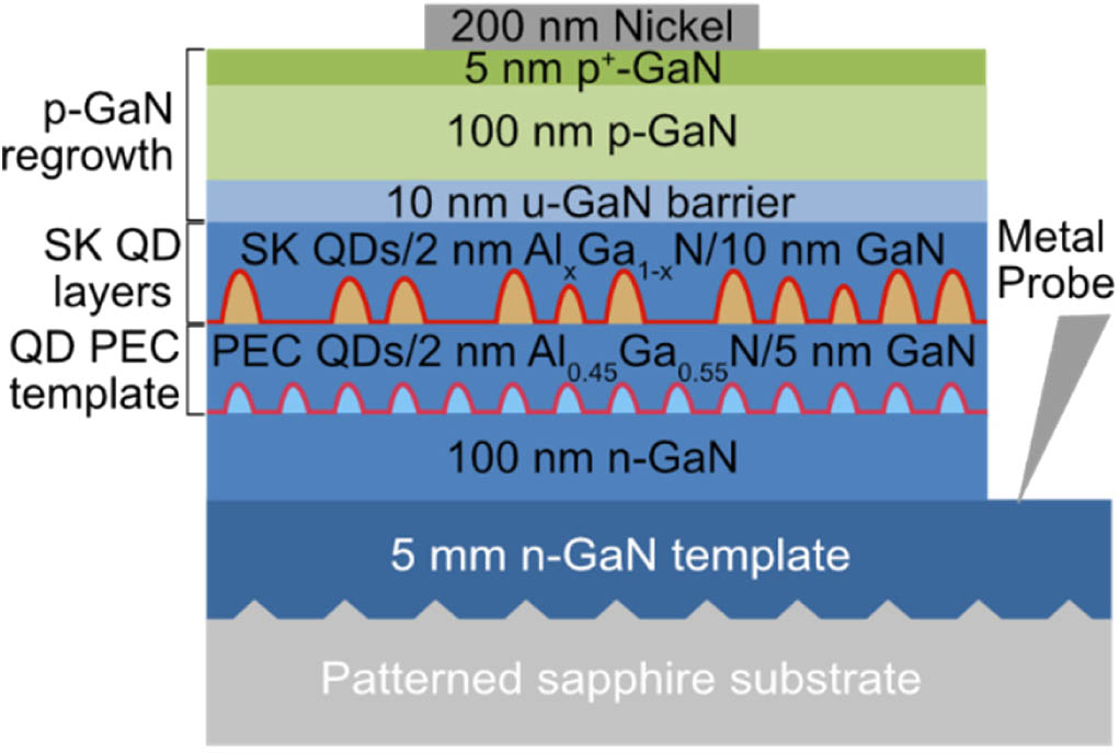
    Fig. 1. Schematic cross section of the entire LED structure consisting of Stranski–Krastanov (SK) quantum dots (QDs) grown on photoelectrochemical (PEC) etched QD templates. Both QD layers are capped with AlGaN layers to protect the QDs. The p-GaN contact is formed by Ni evaporation through a shadow mask, and an electrical “flash” process creates the n-contact.
    Atomic force microscope (AFM) images of a PEC QD template at different synthesized steps: (a) PEC QDs after etching, (b) PEC QDs with Al0.45Ga0.55N grown at 730°C and annealed at 880°C, and (c) PEC QDs with Al0.45Ga0.55N grown at 730°C and GaN barrier grown at 880°C. The AFM images demonstrate that Al0.45Ga0.55N can protect the PEC QDs against collapse.
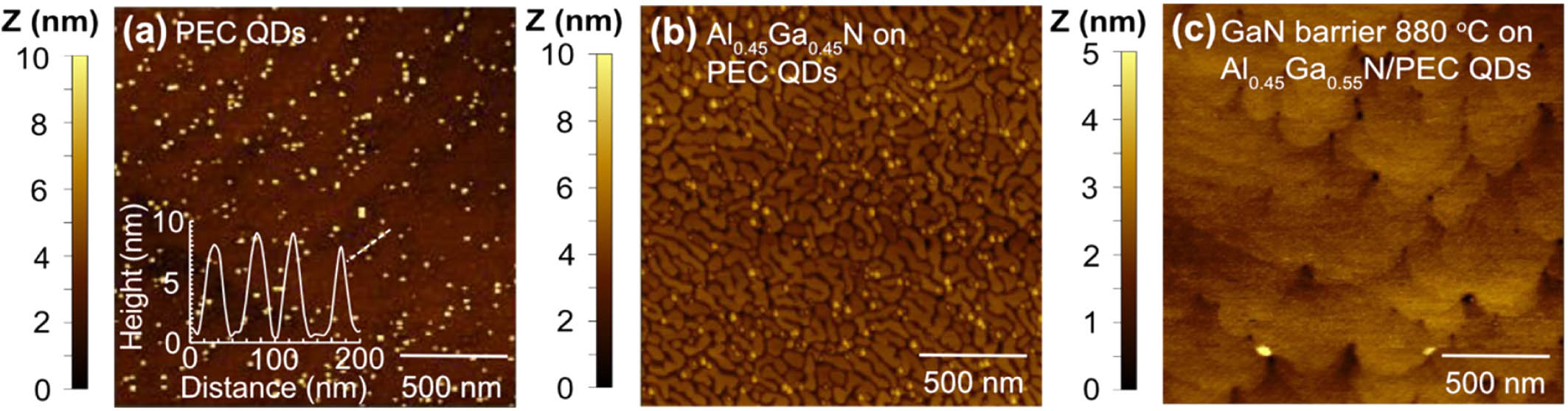
    Fig. 2. Atomic force microscope (AFM) images of a PEC QD template at different synthesized steps: (a) PEC QDs after etching, (b) PEC QDs with Al0.45Ga0.55N grown at 730°C and annealed at 880°C, and (c) PEC QDs with Al0.45Ga0.55N grown at 730°C and GaN barrier grown at 880°C. The AFM images demonstrate that Al0.45Ga0.55N can protect the PEC QDs against collapse.
    AFM images of SK QDs grown on a PEC QD template and with Al0.1Ga0.9N capping and GaN barrier layers. Surfaces of (a) SK InGaN QDs grown at 655°C, (b) SK InGaN QDs capped with Al0.1Ga0.9N grown at 655°C and annealed at 880°C, and (c) SK InGaN QDs with an Al0.1Ga0.9N capping layer grown at 655°C and GaN barrier grown at 880°C. STEM images at (d) 20 nm and (e) 10 nm scale. STEM images show that PEC QDs remain intact, but SK QDs collapse into a QW-like layer due to the insufficient capping and the 880°C GaN barrier growth.
    Fig. 3. AFM images of SK QDs grown on a PEC QD template and with Al0.1Ga0.9N capping and GaN barrier layers. Surfaces of (a) SK InGaN QDs grown at 655°C, (b) SK InGaN QDs capped with Al0.1Ga0.9N grown at 655°C and annealed at 880°C, and (c) SK InGaN QDs with an Al0.1Ga0.9N capping layer grown at 655°C and GaN barrier grown at 880°C. STEM images at (d) 20 nm and (e) 10 nm scale. STEM images show that PEC QDs remain intact, but SK QDs collapse into a QW-like layer due to the insufficient capping and the 880°C GaN barrier growth.
    AFM images of SK QDs with an Al0.9Ga0.1N capping layer grown at 655°C and GaN barrier grown at (a) 855°C and (b) 880°C. AFM images show that at an 855°C GaN growth temperature, the Al0.9Ga0.1N capping layer protects the SK QDs, but the following GaN barrier grows conformally on the SK QDs. The GaN barrier grown at 880°C planarizes the surface.
    Fig. 4. AFM images of SK QDs with an Al0.9Ga0.1N capping layer grown at 655°C and GaN barrier grown at (a) 855°C and (b) 880°C. AFM images show that at an 855°C GaN growth temperature, the Al0.9Ga0.1N capping layer protects the SK QDs, but the following GaN barrier grows conformally on the SK QDs. The GaN barrier grown at 880°C planarizes the surface.
    STEM images of SK QDs capped with an Al0.9Ga0.1N layer and with a GaN barrier grown at 880°C shown at (a) 20 nm, (b) 10 nm, and (c) 5 nm scale. The images show that SK QDs grow on top of the PEC QDs, and the Al0.45Ga0.55N barrier and Al0.9Ga0.1N barrier can protect the PEC QDs and SK QDs, respectively, from collapse at the 880°C growth temperature. (d) EDS image of the sample showing the existence of a wetting layer (orange) below the SK QDs.
    Fig. 5. STEM images of SK QDs capped with an Al0.9Ga0.1N layer and with a GaN barrier grown at 880°C shown at (a) 20 nm, (b) 10 nm, and (c) 5 nm scale. The images show that SK QDs grow on top of the PEC QDs, and the Al0.45Ga0.55N barrier and Al0.9Ga0.1N barrier can protect the PEC QDs and SK QDs, respectively, from collapse at the 880°C growth temperature. (d) EDS image of the sample showing the existence of a wetting layer (orange) below the SK QDs.
    Electroluminescence measurement of the QD LED. (a) Voltage, external quantum efficiency (EQE), and light power versus current of the QD LED. The threshold voltage is <2 V, and the differential resistance is ∼25 Ω. As the current increases, the EQE increases linearly at low current density and slows down at high current density. (b) Spectrum of the QD LED under different currents. The wavelength blueshifts from 800 nm to 500 nm as the current increases. The inset is the spectrum in a linear scale demonstrating a full width at half maximum of 86 nm at 150 mA.
    Fig. 6. Electroluminescence measurement of the QD LED. (a) Voltage, external quantum efficiency (EQE), and light power versus current of the QD LED. The threshold voltage is <2V, and the differential resistance is 25  Ω. As the current increases, the EQE increases linearly at low current density and slows down at high current density. (b) Spectrum of the QD LED under different currents. The wavelength blueshifts from 800 nm to 500 nm as the current increases. The inset is the spectrum in a linear scale demonstrating a full width at half maximum of 86 nm at 150 mA.
    (a) Simulated peak wavelength and wave function overlap squared of the ground state transitions versus carrier screening for a single In0.25Ga0.75N QD capped with a 2 nm thick Al0.9Ga0.1N layer. The QD is hexagonal in shape and surrounded by GaN. The peak wavelength blueshifts with increased carrier screening. Band diagrams and wave functions squared in the vertical direction through the center of the QD for (b) 100% and (c) 0% carrier screening. The wave functions shift from the top and bottom of the QD with no screening to the center with full carrier screening.
    Fig. 7. (a) Simulated peak wavelength and wave function overlap squared of the ground state transitions versus carrier screening for a single In0.25Ga0.75N QD capped with a 2 nm thick Al0.9Ga0.1N layer. The QD is hexagonal in shape and surrounded by GaN. The peak wavelength blueshifts with increased carrier screening. Band diagrams and wave functions squared in the vertical direction through the center of the QD for (b) 100% and (c) 0% carrier screening. The wave functions shift from the top and bottom of the QD with no screening to the center with full carrier screening.
    Xiongliang Wei, Syed Ahmed Al Muyeed, Haotian Xue, Elia Palmese, Renbo Song, Nelson Tansu, Jonathan J. Wierer. Near-infrared electroluminescence of AlGaN capped InGaN quantum dots formed by controlled growth on photoelectrochemical etched quantum dot templates[J]. Photonics Research, 2022, 10(1): 33
    Download Citation