
Peiwen Yuan, Teng Zhang, Jiatao Sun, Liwei Liu, Yugui Yao, Yeliang Wang. Recent progress in 2D group-V elemental monolayers: fabrications and properties[J]. Journal of Semiconductors, 2020, 41(8): 081003
- Journal of Semiconductors
- Vol. 41, Issue 8, 081003 (2020)
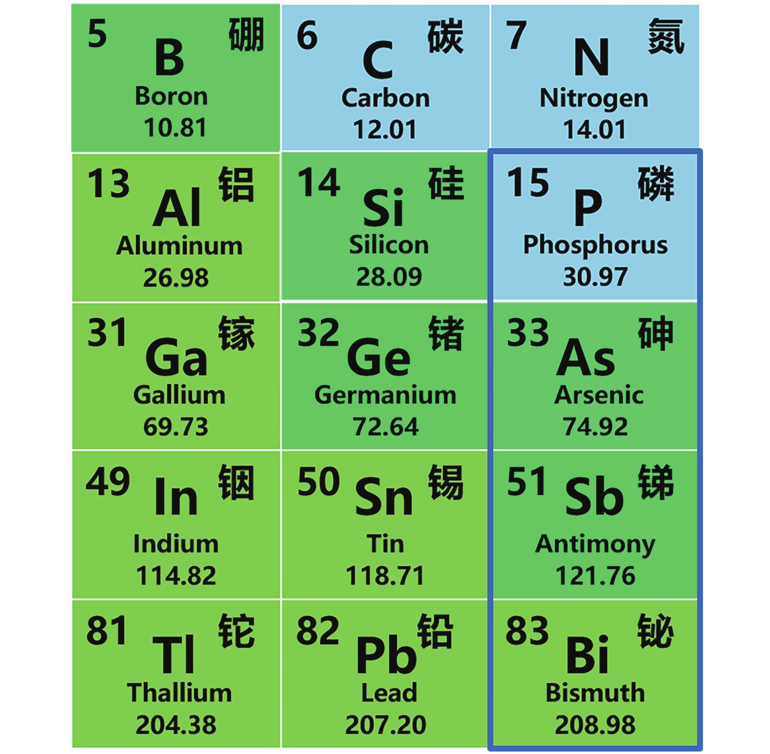
Fig. 1. (Color online) Group-V elements in the period table. Among group-V elements, phosphorus, arsenic, antimony and bismuth (highlighted by blue-frame) are contributed to the formation of 2D monolayer materials phosphorene, arsenene, antimonene and bismuthene, respectively.
![(Color online) (a) The atomic structures of monolayer black phosphorus (BP). The unit cells are highlighted by the black rectangle. a1 and a2 represent the armchair edge and zigzag edge, respectively. (b, c) Electronic band dispersion of monolayer and five-layer BP, respectively. (d) Schematic illustration of preparing BP nanoparticles in water. (e) TEM image of BP nanosheets. (f) SEM images of exfoliated and deposited BP nanosheets. (g) The atomic structures of monolayer blue phosphorus. (h, i) Large-scale and high-resolution STM images of single layer phosphorus on Au(111), respectively. The unit cell in (i) is highlighted by yellow rhombus. (j, k) Calculated band structures of the perfect and spin-polarized SV-(5|9) defective blue phosphorene, respectively. (l) Spin density distribution for SV-(5|9). The yellow and blue colors represent the majority (positive) and the minority (negative) densities, respectively. (a, g–i) reproduced from Ref. [39] from American Chemical Society, copyright 2016; (b, c) reproduced from Ref. [28] from Scientific Citation Index, copyright 2015. (d–f) reproduced from Ref. [33] from Royal Society of Chemistry, copyright 2019. (j–l) reproduced from Ref. [40] from Scientific Citation Index, copyright 2020.](/richHtml/jos/2020/41/8/081003/img_2.jpg)
Fig. 2. (Color online) (a) The atomic structures of monolayer black phosphorus (BP). The unit cells are highlighted by the black rectangle. a 1 and a 2 represent the armchair edge and zigzag edge, respectively. (b, c) Electronic band dispersion of monolayer and five-layer BP, respectively. (d) Schematic illustration of preparing BP nanoparticles in water. (e) TEM image of BP nanosheets. (f) SEM images of exfoliated and deposited BP nanosheets. (g) The atomic structures of monolayer blue phosphorus. (h, i) Large-scale and high-resolution STM images of single layer phosphorus on Au(111), respectively. The unit cell in (i) is highlighted by yellow rhombus. (j, k) Calculated band structures of the perfect and spin-polarized SV-(5|9) defective blue phosphorene, respectively. (l) Spin density distribution for SV-(5|9). The yellow and blue colors represent the majority (positive) and the minority (negative) densities, respectively. (a, g–i) reproduced from Ref. [39 ] from American Chemical Society, copyright 2016; (b, c) reproduced from Ref. [28 ] from Scientific Citation Index, copyright 2015. (d–f) reproduced from Ref. [33 ] from Royal Society of Chemistry, copyright 2019. (j–l) reproduced from Ref. [40 ] from Scientific Citation Index, copyright 2020.
Fig. 3. (Color online) (a) Top view and (b) side view of a buckled As monolayer (arsenene). (c) The band structures of arsenene with respect to external tensile strain, while the red section denotes the contribution of s-type orbital and the blue section means the contribution of p-type orbital. (d, e) Visual comparison between final product of the aqueous shear exfoliation process (AsSE) and starting materials (bulk arsenic). (f) TEM image of shear-exfoliated arsenic nanosheets. (a, b) reproduced from Ref. [21 ] from Wiley, copyright 2015; (c) reproduced from Ref. [41 ] from Institute of Physics Publishing, copyright 2016; (d–f) reproduced from Ref. [42 ] from Wiley, copyright 2017.
Fig. 4. (Color online) (a) Schematic of fabrication process of buckled monolayer antimonene. (b) STM topographic image of large antimonene island on PdTe2. Inset: LEED pattern of antimonene on PdTe2. (c) Atomic resolution STM image of monolayer antimonene. (d) Top view (upper) and side view (lower) of the buckled antimonene. (e) A height profile, showing that the apparent height of the antimonene island. (f) Top view of the overall electron localization function (ELF) of the relaxed model, showing the continuity of the monolayer antimonene. (g) ELF of the cross section, demonstrating high localization of the electrons in Sb–Sb pairs. Typical STM image of antimonene islands on PdTe2 substrate before air exposure in (h), after exposing to air for 20 min in (i), and after 380 K annealing in (j), respectively. Reproduced from Ref. [46 ]. Copyright 2017, Wiley.
Fig. 5. (Color online) (a) Atomic structure and s , p -orbital projected band structure of buckled antimonene in (a) and flat antimonene in (b), in which the shade circles denote the Dirac cone from the out-of-plane p z orbitals. (c) Schematic of fabrication process of flat antimonene. LEED pattern of a clean Ag(111) substrate in (d) and antimonene film on Ag(111) in (e). (f) Large scale STM image of monolayer antimonene on the Ag(111). Inset: A height profile along the line at the terrace edge. (g) High-resolution STM image of antimonene. (h) Line profile revealing the periodicity of the antimonene lattice (5.01 Å). (i) A typical STM image of antimonene island on Ag(111). (j) The apparent height of the island. (k) Top view of the overall electron localization function (ELF) of the relaxed model of FAM. (l) Cross-sectional ELF along the black-dashed line in (k). Reproduced from Ref. [50 ] from American Chemical Society, copyright 2018.
Fig. 6. (Color online) (a) LEED pattern of the SiC(0001)-H substrate, an unreconstructed (1 × 1) surface results from the hydrogenation of the top-layer Si dangling bonds. (b) After Bi deposition, (
I /dV data across the same step. The dI /dV signal of the in-gap states peaks at both film edges (gray dashed lines mark dI /dV maxima). (j) Topographic z (x ) line profile of the step and dI /dV signal of bismuthene (integrated over the gap from +0.15 to +0.55 eV), showing an exponential decrease away from the step edge, on either side. Reproduced from Ref. [53 ]. Copyright 2017, American Association for the Advancement of Science.

Set citation alerts for the article
Please enter your email address
© Copyright 2018-2021 | Chinese Laser Press. All Rights Reserved 沪ICP备15018463号-20