
Peiwen Yuan, Teng Zhang, Jiatao Sun, Liwei Liu, Yugui Yao, Yeliang Wang. Recent progress in 2D group-V elemental monolayers: fabrications and properties[J]. Journal of Semiconductors, 2020, 41(8): 081003
- Journal of Semiconductors
- Vol. 41, Issue 8, 081003 (2020)
Abstract
1. Introduction
Two-dimensional (2D) materials are a kind of monolayer or fewer layer materials whose thickness is much smaller than the lateral dimension. Many of them have novel electronic[
Different from the small bandgap materials, 2D monolayers of group-V elements are semiconductors with significant fundamental bandgaps, which have unique and promising electrical transport properties[
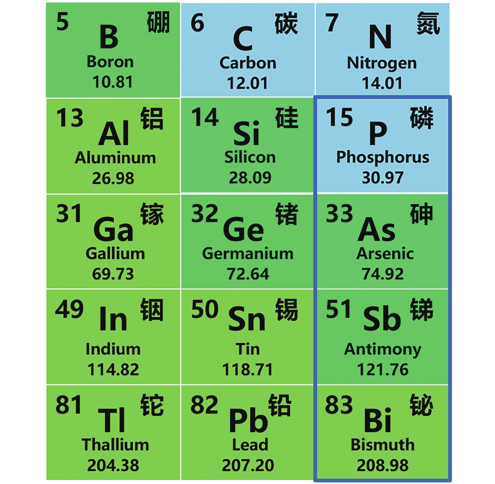
![]()
Figure 1.(Color online) Group-V elements in the period table. Among group-V elements, phosphorus, arsenic, antimony and bismuth (highlighted by blue-frame) are contributed to the formation of 2D monolayer materials phosphorene, arsenene, antimonene and bismuthene, respectively.
This review will sum up the latest progress on 2D group-V materials (phosphorene, arsenene, antimonene and bismuthene), especially the fabrication of group-V monolayers and their fundamental properties and applications. Finally, we will give a perspective on 2D group-V elemental semiconductors.
2. Fabrications and electronic structures of group-V monolayers
2.1. Phosphorene
As a popular element in the Elemental Period Table, phosphorus has white, red, black and several other amorphous forms[
![]()
Figure 2.(Color online) (a) The atomic structures of monolayer black phosphorus (BP). The unit cells are highlighted by the black rectangle.
Blue phosphorus, which was first introduced as “phosphorene”[
2.2. Arsenene
The metallic feature of multilayered arsenic is preserved until the thickness is decreased to a bilayer with a bandgap of 0.37eV, and to monolayer arsenene with a wide bandgap of 2.49 eV, predicted from density-function-theory (DFT) calculations in 2015[
![]()
Figure 3.(Color online) (a) Top view and (b) side view of a buckled As monolayer (arsenene). (c) The band structures of arsenene with respect to external tensile strain, while the red section denotes the contribution of s-type orbital and the blue section means the contribution of p-type orbital. (d, e) Visual comparison between final product of the aqueous shear exfoliation process (AsSE) and starting materials (bulk arsenic). (f) TEM image of shear-exfoliated arsenic nanosheets. (a, b) reproduced from Ref. [
So far, although the synthesis of buckled arsenene with monolayer thickness has not reported experimentally, a large amount of efforts has been paid to fabricate arsenene sheet in experiment. In 2017, Tsai et al. fabricated multilayer arsenene on InAs by the plasma-assisted method[
Besides the plasma-assisted method, it has been recently reported that a high-yield arsenic nanosheets can be prepared by the method of aqueous shear exfoliation[
Figs. 3(d) and 3(e) show the comparison between the starting materials and the final product of the shear exfoliation process. By using transmission electron microscope (TEM), the morphology of exfoliated arsenic nanosheets were shown in Fig. 3(f). The achieved arsenic nanosheets has visible wrinkled structure, which consists of few-layer materials. In addition, using the dynamic light scattering, the particles with diameters of arsenic nanosheets was investigated, which ranges between 100–200 nm dominantly.
2.3. Antimonene
2.3.1. Epitaxial growth of buckled monolayer antimonene
Antimonene, which was predicted to have a bandgap of 2.28 eV[
The fabrication process of monolayer antimonene is illustrated in Fig. 4(a). The antimony atoms were evaporated from a Knudsen crucible and deposited onto a pre-cleaved PdTe2 substrate kept at 400 K. Fig. 4(b) is a typical topographic image of as-resulted antimonene in a large-scale with a well-ordered LEED pattern inset, showing the high quality of the antimonene adlayer on the PdTe2 substrate. Fig. 4(c) is a high-resolution STM image of antimonene adlayer, demonstrating a graphene-like honeycomb lattice of the antimonene. In addition, a buckled configuration of this honeycomb lattice can be seen in Fig. 4(d). Moreover, the periodicity of this honeycomb lattice is 4.13 ± 0.02 Å, which is quite close to the lattice constant of the PdTe2 substrate (4.10 ± 0.02 Å). Therefore, this close match of these two lattices consistent with the LEED pattern showing (1 × 1) diffraction points (inset in Fig. 4(b)). The apparent height of antimonene is 2.8 Å (Fig. 4(e)), showing that the antimonene adlayer is a monolayer. A relaxed model with calculated electron localization function (ELF) value of 0.6 is shown in Fig. 4(f), illustrating the continuity of the adlayer antimonene.
![]()
Figure 4.(Color online) (a) Schematic of fabrication process of buckled monolayer antimonene. (b) STM topographic image of large antimonene island on PdTe2. Inset: LEED pattern of antimonene on PdTe2. (c) Atomic resolution STM image of monolayer antimonene. (d) Top view (upper) and side view (lower) of the buckled antimonene. (e) A height profile, showing that the apparent height of the antimonene island. (f) Top view of the overall electron localization function (ELF) of the relaxed model, showing the continuity of the monolayer antimonene. (g) ELF of the cross section, demonstrating high localization of the electrons in Sb–Sb pairs. Typical STM image of antimonene islands on PdTe2 substrate before air exposure in (h), after exposing to air for 20 min in (i), and after 380 K annealing in (j), respectively. Reproduced from Ref. [
Fig. 4(g) is a cross-section ELF pattern perpendicular to the monolayer antimonene, which is corresponded to the black line in Fig. 4(f). This image clearly shows two important EFL ranges: the ELF value of the Sb–Sb pair is larger than 0.8 and the ELF value of the strongest coupling region between the antimonene and substrate is less than 0.3. The comparison of these EFL ranges demonstrates that a strong interaction exists within the antimonene and a weak interaction exists between antimonene and PdTe2 substrate.
The environmental stability of atomic-thickness 2D materials is of great importance. STM images of the sample before and after exposed in the air were shown in Figs. 4(h) and 4(i), which reveal that the antimonene island are clean without any impurity on the islands. Moreover, after annealing the sample at 380 K, the STM image of antimonene island (Fig. 4(j)) is quite similar to the initial state image. This evidence strongly proves the monolayer antimonene is quite inert to air. More recently, topological edge states have been found in buckled antimonene islands on top of antimonene monolayers, which is promising for future low-power electronic nanodevices and quantum computations[
2.3.2. Epitaxial growth of flat antimonene monolayer
Compared to monolayer graphene with flat honeycomb lattice, group-V monolayer materials usually have a buckled structure. Interestingly, flat antimonene monolayer (FAM) is theoretically predicted and also realized by MBE growth, as reported by Shao et al. in 2018[
Theoretically, the s-orbital and p-orbital projected band structure of the buckled antimonene are calculated, as shown in Fig. 5(a). The hybridized bands around the Fermi level between the s, px, py, pz orbitals of the Sb atom lead to the partially hybridized sp3 bands. As for the flat antimonene, there is no mutual hybridization between in-plane orbitals and out-of-plane ones as shown in Fig. 5(b). The in-plane orbitals lead to a hybridized sp2 band. The out-of-plane orbitals lead to the Dirac cone of π bands resembling that of graphene around the Fermi level as denoted by the gray circles.
![]()
Figure 5.(Color online) (a) Atomic structure and
Experimentally, antimony atoms were deposited onto a pre-clean Ag(111) substrate kept at a relative low temperature of 353 K. A well-organized antimonene adlayer was formed on the substrate. Fig. 5(d) showed LEED pattern of the clean Ag(111) substrate with sharp (1 × 1) diffraction spots. Fig. 5(e) showed LEED pattern of the antimonene on the substrate, showing a (
A typical STM image of the antimonene adlayer is shown in Fig. 5(f), revealing a uniform film on the substrate. Fig. 5(g) is the close-up STM image of the sample, showing a clear honeycomb-like lattice. Measured along the profile line in Fig. 5(g), the period of 5.01 Å for the antimonene was obtained, which is consistent with the superstructure observed in the LEED patterns. Moreover, the height of the antimonene film is 2.2 Å, as shown in Fig. 5(h), which is lower than the buckled monolayer antimonene (2.8 Å)[
Moreover, to determine whether Sb–Sb chemical bond exists in the flat configuration, the ELF of the antimonene monolayer on Ag(111) was carried out. Fig. 5(k) is the top view of the ELF for the optimized model of FAM, revealing the continuity of the antimonene. Along the black-line in Fig. 5(l) is the cross-sectional ELF, the different colors in different regions represent different interaction, suggesting strong chemical bond of the Sb-Sb pairs and weak Sb–Ag interaction. As for the configuration of this flat honeycomb lattice of FAM, it is sustained by the substrate. So, it is important to exfoliate these antimonene films from the substrate for its practical applications in the future, which need further exploring.
2.4. Bismuthene
Given antimonene with the bandgap of 2.28 eV[
In Reis’s work, the use of SiC(0001) as the substrate is vital because this substrate is not only stabilizing the bismuthene as a quasi-2D topological insulator but also playing a great role in achieving a large gap. N-doped Si-terminated 4H-SiC substrate was first dry-etched in a hydro-based gas atmosphere at a temperature of ~1230 °C. And then the H-termination of the substrate was removed by a slow thermal H desorption at ~650 °C while immediately offer Bi atoms on the substrate. The substrate was then lowered to ~500 °C to condense Bi layer, then a
![]()
Figure 6.(Color online) (a) LEED pattern of the SiC(0001)-H substrate, an unreconstructed (1 × 1) surface results from the hydrogenation of the top-layer Si dangling bonds. (b) After Bi deposition, (
To establish the electronic structure of the bismuthene material, Reis et al. decomposed the band structure into σ-bond contributions came from Bi 6s, px, py orbitals and π-bond contribution from pz orbitals. The orbitals at low energy are mainly σ bands, as shown in Fig. 6(e), as the hybridization of bismuthene and substrate is via π bonds. Considering the electronic structure around EF, for the low energy bands without spin-orbital coupling (SOC), there is a Dirac-like band crossing at the K point, as shown in Fig. 6(f). However, when considering a strong atomic SOC, there is a large bandgap at the K point (Fig. 6(g)), and the Rashba term λR can lift the degeneracy of the valence-band and induces the spin-degenerate of the conduction band at K point (Fig. 5(h)). By using scanning tunneling spectroscopy (STS), the differential tunneling conductivity (dI/dV) curves show that while the interior of the island shows insulating gap feature, conductive states exists at the edges (Figs. 6(i) and 6(j)), which suggests that QSH exists in bismuthene/SiC. More excitingly, the bulk gap of bismuthene is up to 0.8 eV, which makes it a candidate for a high-temperature quantum spin Hall material. Very recently, the strong interaction electrons at the edge of the bismuthene on SiC(0001) was also reported to exhibit Luttinger liquid feature, providing a new platform to study one-dimensional electronic feature[
3. Summary and perspectives
There has been enormous progress on the study of group-V monolayers, especially on the preparation of new members and structural tuning of new materials. Phosphorene, which has amounts of excellent properties, such as tunable direct gap, high carrier mobility has been successfully fabricated on a Au(111) substrate by MBE. Arsenic nanosheets have been successfully prepared by aqueous shear exfoliation, which has visible wrinkled structure consisting of few-layer materials. As for antimonene, high quality buckled antimonene monolayer has been successfully grown on a PdTe2 substrate, which represented excellent air stability in ambient environment. Moreover, flat antimonene monolayer has been also successfully fabricated on a Ag (111) substrate by MBE, which holding tunable topological properties for future applications. Regarding bismuthene, flat configuration as a two-dimensional topological insulator (2DTI) was experimentally obtained on a SiC (0001) substrate, with a large SOC gap, making it a candidate for a high-temperature quantum spin Hall material.
Undoubtedly, the experimental realization of group-V monolayers extend the scope of 2D atomically-thick structure and pave a way for the future application in spintronics. However, there are still some drawbacks in above-mentioned works on 2D monoelemental group-V monolayer materials. (1) Until now, the synthesis of buckled arsenene with monolayer thickness, which was predicted theoretically a wide bandgap, is not reported experimentally. (2) The flat antimonene monolayer films by MBE method are not electrically isolated from the metal substrate. (3) The excited findings are that the intriguing topological properties of group-V monolayers are reported experimentally in both antimonene and bismuthene monolayer, however, the low-energy-cost devices, based on the topological property of group-V monolayer, are still lacking, although there reported a lot of optoelectronic devices utilizing the semiconductor properties. So, there are many opportunities for research to exploit the structural controlling and potential applications in functional nanodevices. We hope that this review will inspire more attempts and findings in the group-V families, and we believe that related challenges can be solved in the near future.
Acknowledgements
Thanks the financial supporting from National Natural Science Foundation of China (Nos. 61971035, 61901038, 61725107), Beijing Natural Science Foundation (Nos. Z190006, 4192054), Strategic Priority Research Program of the Chinese Academy of Sciences (XDB30000000), and Beijing Institute of Technology Research Fund Program for Young Scholars (3050011181814).
References
[1] G Fiori, F Bonaccorso, G Iannaccone et al. Electronics based on two-dimensional materials. Nat Nanotechnol, 9, 768(2014).
[2] K S Novoselov, A Mishchenko, A Carvalho et al. 2D materials and van der Waals heterostructures. Science, 353, aac9439(2016).
[3] G Li, Y Y Zhang, H Guo et al. Epitaxial growth and physical properties of 2D materials beyond graphene: From monatomic materials to binary compounds. Chem Soc Rev, 47, 6073(2018).
[4] M Gibertini, M Koperski, A F Morpurgo et al. Magnetic 2D materials and heterostructures. Nat Nanotechnol, 14, 408(2019).
[5] J B Cheng, C L Wang, X M Zou et al. Recent advances in optoelectronic devices based on 2D materials and their heterostructures. Adv Opt Mater, 7, 1800441(2019).
[6] I Epstein, A J Chaves, D A Rhodes et al. Highly confined in-plane propagating exciton-polaritons on monolayer semiconductors. 2D Mater, 7, 035031(2020).
[7] J Kou, E P Nguyen, A Merkoçi et al. 2-dimensional materials-based electrical/optical platforms for smart on-off diagnostics applications. 2D Mater, 7, 032001(2020).
[8] X Lin, J C Lu, Y Shao et al. Intrinsically patterned two-dimensional materials for selective adsorption of molecules and nanoclusters. Nat Mater, 16, 717(2017).
[9] X H Niu, Y W Yi, L J Meng et al. Two-dimensional phosphorene, arsenene, and antimonene quantum dots: Anomalous size-dependent behaviors of optical properties. J Phys Chem C, 123, 25775(2019).
[10] Y Zhang, T R Chang, B Zhou et al. Direct observation of the transition from indirect to direct bandgap in atomically thin epitaxial MoSe2. Nat Nanotechnol, 9, 111(2014).
[11] S Das Sarma, S Adam, E H Hwang et al. Electronic transport in two-dimensional graphene. Rev Mod Phys, 83, 407(2011).
[12] C C Liu, W X Feng, Y G Yao. Quantum spin Hall effect in silicene and two-dimensional germanium. Phys Rev Lett, 107, 076802(2011).
[13] Z H Wu, J H Hao. Electrical transport properties in group-V elemental ultrathin 2D layers. npj 2D Mater Appl, 4, 4(2020).
[14] S L Zhang, S Y Guo, Z F Chen et al. Recent progress in 2D group-VA semiconductors: From theory to experiment. Chem Soc Rev, 47, 982(2018).
[15] G Z Qin, Z Z Qin. Negative Poisson's ratio in two-dimensional honeycomb structures. npj Comput Mater, 6, 51(2020).
[16] Y Q Ma, C F Shen, A Zhang et al. Black phosphorus field-effect transistors with work function tunable contacts. ACS Nano, 11, 7126(2017).
[17] R X Fei, L Yang. Strain-engineering the anisotropic electrical conductance of few-layer black phosphorus. Nano Lett, 14, 2884(2014).
[18] Q Liu, X W Zhang, L Abdalla et al. Switching a normal insulator into a topological insulator via electric field with application to phosphorene. Nano Lett, 15, 1222(2015).
[19] J S Qiao, X H Kong, Z X Hu et al. High-mobility transport anisotropy and linear dichroism in few-layer black phosphorus. Nat Commun, 5, 4475(2014).
[20] L T T Phuong, T C Phong, M Yarmohammadi. Spin-splitting effects on the interband optical conductivity and activity of phosphorene. Sci Rep, 10, 9201(2020).
[21] S L Zhang, Z Yan, Y F Li et al. Atomically thin arsenene and antimonene: Semimetal-semiconductor and indirect-direct band-gap transitions. Angew Chem Int Ed, 54, 3112(2015).
[22] M Wada, S Murakami, F Freimuth et al. Localized edge states in two-dimensional topological insulators: Ultrathin Bi films. Phys Rev B, 83, 121310(2011).
[23] S Murakami. Quantum spin Hall effect and enhanced magnetic response by spin-orbit coupling. Phys Rev Lett, 97, 236805(2006).
[24] A Brown, S Rundqvist. Refinement of the crystal structure of black phosphorus. Acta Crystallogr, 19, 684(1965).
[25] H Thurn, H Kerbs. Crystal structure of violet phosphorus. Angew Chem Int Ed, 5, 1047(1966).
[26] R Hultgren, N S Gingrich, B E Warren. The atomic distribution in red and black phosphorus and the crystal structure of black phosphorus. J Chem Phys, 3, 351(1935).
[27] S Appalakondaiah, G Vaitheeswaran, S Lebègue et al. Effect of van der Waals interactions on the structural and elastic properties of black phosphorus. Phys Rev B, 86, 035105(2012).
[28] S Fukuoka, T Taen, T Osada. Electronic structure and the properties of phosphorene and few-layer black phosphorus. J Phys Soc Jpn, 84, 121004(2015).
[29] L B Liang, J Wang, W Z Lin et al. Electronic bandgap and edge reconstruction in phosphorene materials. Nano Lett, 14, 6400(2014).
[30] J S Kim, P J Jeon, J Lee et al. Dual gate black phosphorus field effect transistors on glass for NOR logic and organic light emitting diode switching. Nano Lett, 15, 5778(2015).
[31] M Buscema, D J Groenendijk, S I Blanter et al. Fast and broadband photoresponse of few-layer black phosphorus field-effect transistors. Nano Lett, 14, 3347(2014).
[32] L K Li, Y J Yu, G J Ye et al. Black phosphorus field-effect transistors. Nat Nanotechnol, 9, 372(2014).
[33] A R Baboukani, I Khakpour, V Drozd et al. Single-step exfoliation of black phosphorus and deposition of phosphorene via bipolar electrochemistry for capacitive energy storage application. J Mater Chem, 7, 25548(2019).
[34] H Liu, A T Neal, Z Zhu et al. Phosphorene: an unexplored 2D semiconductor with a high hole mobility. ACS Nano, 8, 4033(2014).
[35] J Xie, M Si, D Yang et al. A theoretical study of blue phosphorene nanoribbons based on first-principles calculations. J Appl Phys, 116, 073704(2014).
[36] Y Aierken, D Cakir, C Sevik et al. Thermal properties of black and blue phosphorenes from a first-principles quasiharmonic approach. Phys Rev B, 92, 081408(2015).
[37] B Ghosh, S Nahas, S Bhowmick et al. Electric field induced gap modification in ultrathin blue phosphorus. Phys Rev B, 91, 115433(2015).
[38] Z Zhu, D Tománek. Semiconducting layered blue phosphorus: A computational study. Phys Rev Lett, 112, 176802(2014).
[39] J L Zhang, S T Zhao, C Han et al. Epitaxial growth of single layer blue phosphorus: A new phase of two-dimensional phosphorus. Nano Lett, 16, 4903(2016).
[40] C Wang, Y Z You, J H Choi. First-principles study of defects in blue phosphorene. Mater Res Express, 7, 015005(2019).
[41] Y P Wang, C W Zhang, W X Ji et al. Tunable quantum spin Hall effect via strain in two-dimensional arsenene monolayer. J Phys D, 49, 055305(2016).
[42] R Gusmão, Z Sofer, D Bouša et al. Innentitelbild: pnictogen (As, Sb, Bi) nanosheets for electrochemical applications are produced by shear exfoliation using kitchen blenders. Angew Chem Int Ed, 129, 14510(2017).
[43] C Kamal, M Ezawa. Arsenene: Two-dimensional buckled and puckered honeycomb arsenic systems. Phys Rev B, 91, 085423(2015).
[44] G Pizzi, M Gibertini, E Dib et al. Performance of arsenene and antimonene double-gate MOSFETs from first principles. Nat Commun, 7, 12585(2016).
[45] H Tsai, S Wang, C Hsiao et al. Direct synthesis and practical bandgap estimation of multilayer arsenene nanoribbons. Chem Mater, 28, 425(2016).
[46] P Ares, F Aguilar-Galindo, D Rodríguez-San-miguel et al. Mechanical isolation of highly stable antimonene under ambient conditions. Adv Mater, 28, 6332(2016).
[47] J P Ji, X F Song, J Z Liu et al. Two-dimensional antimonene singlecrystals grown by van der Waals epitaxy. Nat Commun, 7, 13352(2016).
[48] X Wu, Y Shao, H Liu et al. Epitaxial growth and air-stability of monolayer antimonene on PdTe2. Adv Mater, 29, 1605407(2017).
[49] S Zhu, Y Shao, E Wang et al. Evidence of topological edge states in buckled antimonene monolayers. Nano Lett, 19, 6323(2019).
[50] Y Shao, Z L Liu, C Cheng et al. Epitaxial growth of flat antimonene monolayer: A new honeycomb analogue of graphene. Nano Lett, 18, 2133(2018).
[51] A D Zhao, B Wang. Two-dimensional graphene-like Xenes as potential topological materials. APL Mater, 8, 030701(2020).
[52] Z Liu, C X Liu, Y S Wu et al. Stable nontrivial Z2 topology in ultrathin Bi (111) films: A first-principles study. Phys Rev Lett, 107, 136805(2011).
[53] F Reis, G Li, L Dudy et al. Bismuthene on a SiC substrate: A candidate for a high-temperature quantum spin Hall material. Science, 357, 287(2017).
[54] R Stühler, F Reis, T Müller et al. Tomonaga–Luttinger liquid in the edge channels of a quantum spin Hall insulator. Nat Phys, 16, 47(2020).

Set citation alerts for the article
Please enter your email address
© Copyright 2018-2021 | Chinese Laser Press. All Rights Reserved 沪ICP备15018463号-20