
Hong Zhou, Jincheng Zhang, Chunfu Zhang, Qian Feng, Shenglei Zhao, Peijun Ma, Yue Hao. A review of the most recent progresses of state-of-art gallium oxide power devices[J]. Journal of Semiconductors, 2019, 40(1): 011803
- Journal of Semiconductors
- Vol. 40, Issue 1, 011803 (2019)
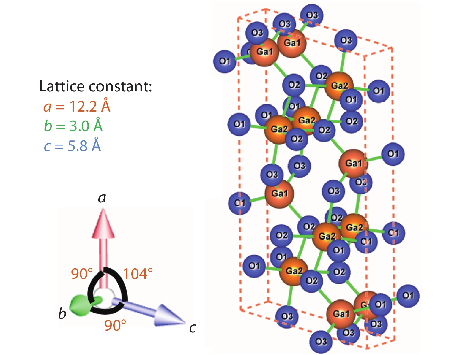
Fig. 1. (Color online) Atomic unit cell of β -Ga2O3 with lattice constant and angle marked.
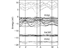
Fig. 2. Band structure of β -Ga2O3 with Fermi energy aligned to zero. Reprint from Appl Phys Lett, 88, 261904 (2006). Copyright 2006 American Institute of Physics.
Fig. 3. Photograph of 4-inch-diameter β -Ga2O3 wafer. Reprinted from Higashiwaki et al. , J Phy D, 50 (2017). Copyright 2017 IOP Publishing[30 ].
Fig. 4. (Color online) β -Ga2O3 crystals grown by the VB method in either (a) a full-diameter crucible (a’), and (b) or in a conical crucible (b’). Reprinted from Hoshikawa et al. , J Cryst Growth 447, 36 (2016). Copyright 2016 Elsevier[31 ].
Fig. 5. (Color online) (a) HRTEM image of an undoped homoepitaxial β -Ga2O3 layer from MOVPE method. (b) Surface morphologies of 60-nm-thick β -Ga2O3 (010) layers grown on Sn-doped β -Ga2O3 (010) substrates at a growth rate of 1 nm/min under slightly Ga-rich conditions at the growth temperatures of 500, 700, 800, and 900 °C, respectively. NDIC microscopy images of β -Ga2O3 surfaces after HVPE growth on (001) β -Ga2O3 substrates for 1 h at (c) 800 and (d) 1000 °C. Reprinted from Refs. [33 , 37 , 41 ].
Fig. 6. (Color online) (a) Electron mobility as a function of carrier concentration. (b) I–V characteristics of Pt/β -Ga2O3 Schottky barrier diodes. The inset shows the schematic structure of the β -Ga2O3 SBD. Reprinted from Sasaki et al. , Appl Phys Express, 5, 035502 (2012)[52 ]. Copyright of 2012 Japanese Society of Applied Physics.
Fig. 7. (Color online) (a) Forward and (b) reverse J–V characteristics of β -Ga2O3 FP-SBD at room temperature. Inset shows the cross-section device schematic of the vertical SBD. Reprinted from Appl Phys Lett, 110, 103506 (2017). Copyright 2017 American Institute of Physics[53 ].
Fig. 8. (Color online) (a) Reverse I–V characteristics of 3 diodes with two different diameters, showing a diameter dependence of the BV, and (b) forward and reverse I–V characteristics from a 20 μ m diameter diode. Reprinted from Appl Phys Lett, 110, 192101 (2017) and IEEE Electron Device Lett. Copyrights 2017 American Institute of Physics and 2017 IEEE[54 , 55 ].
Fig. 9. (Color online) (a) DC output characteristics of β -Ga2O3 MESFET and (b) transfer characteristics of the same MESFET at V DS = 40 V. Reprinted from Appl Phys Lett, 100, 013504 (2012). Copyrights 2012 American Institute of Physics[57 ].
Fig. 10. (Color online) (a) Schematic cross section of a β -Ga2O3 MOSFET with a gate-connected FP structure and (b) Output characteristics of the MOSFET with maximum I D of 78 mA/mm and BV of 750 V. Reprinted from IEEE Electron Device Lett, 37, 2 (2016). Copyright of 2016 IEEE[58 ].
Fig. 11. (Color online) (a) Cross-section view and (b) optical image of the fabricated field-plated Ga2O3 MOSFET with SOG S/D doping. (c) Three-terminal breakdown measurement of the field-plated Ga2O3 MOSFET and a record-high BV of 1850 V is demonstrated. Reprinted from IEEE Electron Device Lett, 39, 9 (2018). Copyright of 2018 IEEE[59 ].
Fig. 12. (Color online) I D–V GS characteristics of (a) Zeng’s and (b) Tadjer’s E-mode MOSFET. Reprinted from IEEE Device Research Conf and ECS J, Solid State Sci, Technol, 39, 9 (2018). Copyright of 2016 IEEE[60 ] and 2016 ECS[5 ].
Fig. 13. (Color online) (a) Tilted false-colored SEM image of a fabricated E-mode β -Ga2O3 Fin-MOSFET and (b) The breakdown characteristics of β -Ga2O3 Fin-MOSFET with L G = 2 μ m and L GD = 16, 21 μ m at V GS = 0 V. The inset shows the transfer characteristics of the same device indicating a V TH = 0.8 V. Reprinted from Appl Phys Lett, 109, 213501 (2016). Copyrights 2016 American Institute of Physics[4 ].
Fig. 14. (Color online) (a) Schematic cross-section and (b) SEM image of a vertical E-mode β -Ga2O3 Fin-MOSFET, (c) transfer characteristics of the device with a V TH = 2.2 V, on/off ratio of 108, and on-current of 400 A/cm2. (d) The breakdown characteristics of β -Ga2O3 Fin-MOSFET with channel width of 330 nm. Reprinted from IEEE Electron Device Lett, 39, 869, 2018. Copyright of 2018 IEEE[61 ].
Fig. 15. (Color online) (a) A device cross section schematic is shown for the β -Ga2O3 MOSFET under test. (b) A focused ion beam (FIB) cross sectional image of the device. (c) Extrinsic small signal RF gain performance recorded at V GS = −3.5 V (peak gm) and V DS = 40 V (d) 800 MHz Class-A power sweep of a 2 × 50 μ m β -Ga2O3 gate recessed MOSFET. Reprinted from IEEE Electron Device Lett, 38, 790, 2017. Copyright of 2017 IEEE[62 ].
Fig. 16. (Color online) (a) DC output characteristics and pulsed I –V from a quiescent bias of V GS = V DS = 0 V up to V DS = 80 V with 1 μ s pulse length and 1 ms period (b) Pulsed and CW large signal measurements at 1 GHz with input available power sweep up to 22 dBm, measured at V DS = 40 V with I DS = 5 mA. Reprinted from IEEE Electron Device Lett, 39, 1572, 2018. Copyright of 2018 IEEE[63 ].
Fig. 17. (Color online) Transfer characteristics of the thin-channel BGO MOSFET with T-gate. The G M reaches 25 mS/mm with current density over 275 mA/mm, and the inset shows a good I ON/I OFF ratio greater than 108. (b) Small signal gain at V DS = 15 V of the thin-channel BGO MOSFET with f t/f max = 5.1/17.1 GHz. Reprinted from IEEE IMWS-AMP, 2018. Copyright of 2018 IEEE[64 ].
Fig. 18. (Color online) (a) Schematic-view and (b) top-view microscopy image of a fabricated lateral β -Ga2O3 SBD on sapphire substrate. (c) Log-scale forward characteristics of β -Ga2O3 SBD with L Schottky-Ohmic = 15 μ m at the temperature range from 30 to 150 °C with 20 °C as a step. (d) Linear-scale forward I–V characteristics of β -Ga2O3 SBDs with various L Schottky−Ohmic. (e) Reverse I–V characteristics of lateral β -Ga2O3 SBDs with various L Schottky−Ohmic. Reprinted from IEEE JEDS 6, 815, 2018. Copyright of 2018 IEEE[66 ].
Fig. 19. (Color online) (a) Tilted 3-D schematic-view and (b) top-view microscopy image of a fabricated lateral field-plated β -Ga2O3 SBD on Sapphire substrate. (c) Forward I–V and differential R on–V characteristics in linear scale. The inset shows as-measured current dependence on the width of the SBD at a similar L AC of 14–18 μ m. (d) Reverse I–V characteristics of lateral SBDs with field plate structure and various L AC. (e) DC RON,SP versus BV of some both lateral and vertical β -Ga2O3 SBDs. Reprinted from IEEE Electron Device Lett, 39, 1564, 2018. Copyright of 2018 IEEE[51 ].
Fig. 20. (Color online) (a) Schematic view of a GOOI FET with a 300 nm SiO2 layer on Si substrate and (b) AFM image of the atomic flat β -Ga2O3 surface after cleavage. Reprinted from IEEE Electron Device Lett, 38, 103, 2017. Copyright of 2017 IEEE[68 ].
Fig. 21. (Color online) (a) and (c) are I D–V DS output characteristics of D- and E-mode GOOI FETs with 3.0 × 10¹⁸ and 8.0 × 1018 cm−3 doping channel, respectively. (b) and (d) are I D–g m–V GS transfer characteristics of D-mode and E-mode GOOI FETs with 8.0 × 1018 cm−3 doping channel, respectively. Record high I DMAX of 1.5 and 1.0 A/mm are demonstrated for D/E mode devices. Both D and E-mode devices have high on/off ratio of 1010 and low SS of 150–165 mV/dec for 300 nm SiO2. Reprinted from Appl Phys Lett, 111, 092102, 2017. Copyright of 2017 AIP[67 ].
Fig. 22. (Color online) (a) Thickness dependent I D–V GS plots of various GOOI FETs from D-mode of thicker β -Ga2O3 to E-mode of thinner β -Ga2O3. (b) Thickness dependent V T extracted at V DS = 1 V of 15 devices. Reprinted from IEEE Electron Device Lett, 38, 103, 2017. Copyright of 2017 IEEE[68 ].
Fig. 23. (Color online) (a) I D–V GS comparison between GOOI FETs with and without ALD passivation for β -Ga2O3 nano-membrane with doping concentration of 3.0 × 1018 cm−3, (b) simulated C–V curve for E-mode GOOI FET at a β -Ga2O3 nano-membrane thickness of 80 nm and doping concentration of 3.0 × 1018 cm−3 after considering the top and bottom negative surface charge (n s = 1.2 × 1013 cm2) depletion effect. Band diagram and electron density distribution of E-mode GOOI FETs with surface negative charge depletion on (c) lower doping (n s = 1.2 × 1013 cm−2) and (d) high doping (n s = 2.2 × 1013 cm−2) β -Ga2O3 nano-membrane channels at V GS = 0 V. Reprinted from Appl Phys Lett, 111, 092102, 2017. Copyright of 2017 AIP[67 ].
Fig. 24. (Color online) Cross-section schematic view of a top-gate GOOI FET on (a) SiO2/Si and (b) sapphire and diamond substrates with different κ marked. 15 nm of Al2O3 is used as the gate dielectric, Ti/Al/Au (15/60/50 nm) is used as the source/drain electrodes, and Ni/Au (30/50 nm) is used the gate electrode. (c) False-colored SEM top-view of a GOOI FET with L G = 1 μ m and L SD = 6 μ m. Reprinted from ACS Omega 2,11, 2017. Copyright of 2017 ACS[71 ].
Fig. 25. (Color online) I D–V DS characteristics of GOOI FETs on (a) SiO2/Si, (b) sapphire and (c) diamond substrates with L SD = 6–6.5 μ m and L G = 1 μ m. A high I DMAX = 960 mA/mm is demonstrated on top-gate β -Ga2O3 GOOI FETs. Comparison of (d) I D−V DS (e) log-scale I D−V GS and (f) linear-scale g m−V GS of β -Ga2O3 FETs on a diamond, sapphire and SiO2/Si substrates. I D–V GS transfer characteristics of GOOI FETs on three substrates with high on/off ratio of 109 and low SS of 65 mV/dec, yielding a low D it of 2.6 × 10¹¹ eV−1·cm−2. Higher g m shows higher electron μ on diamond due to the reduced device temperature. Reprinted from ACS Omega 2,11, 2017. Copyright of 2017 ACS[71 ] and 2018 IEEE[72 ].
Fig. 26. (Color online) TR and charge-coupled device (CCD) camera merged images of GOOI FET on (a) SiO2/Si, (b) sapphire and (c) diamond substrates when device P is increased by increasing V DS at V GS = 0 V. (d) Comparison of measured or simulated ΔT versus P (W/mm2) characteristics of top-gate GOOI FETs on a diamond substrate using TR imaging, Raman thermography and the thermal simulations. (e) Measured by TR method and simulated ΔT versus P characteristics of top-gate GOOI FETs on different substrates. The ΔT of GOOI FET on the SiO2/Si substrate is more than 3 and 8 times of that on the sapphire and diamond substrates at the same P . As a result, the R T of GOOI FET on the sapphire substrate is 4.62 × 10⁻² and 1.71 × 10⁻² mm2·K/W, which is less than 1/3 and 1/8 of that on the SiO2/Si substrate. Reprinted from ACS Omega 2,11, 2017. Copyright of 2017 ACS[71 ].
Fig. 27. (Color online) (a) Schematic view of β -Ga2O3 FE-FETs. The gate stack includes a heavily n-doped Si as the gate electrode, 20 nm HZO as the ferroelectric insulator, 3 nm Al2O3 as the capping layer. Ti/Au (30/60 nm) is used as the source/drain electrodes. Sn-doped n-type β -Ga2O3 (86 nm) is used as the channel. (b) Top-view false-color SEM image of representative β -Ga2O3 FE-FETs on the same membrane with different channel lengths. (c) Cross-sectional view of the HZO/Al2O3 gate stack, capturing the polycrystalline HZO and the amorphous Al2O3. Reprinted from ACS Omega 2,10, 2017. Copyright of 2017 ACS[74 ].
Fig. 28. (Color online) (a) I D–V GS characteristics in the log scale of a β -Ga2O3 FE-FET. This device has a channel length of 0.5 μ m and a channel thickness of 86 nm. SS versus I D characteristics of the same device in (a) at (b) V DS = 0.1, (c) V DS = 0.5, and (d) V DS = 0.9 V. SS less than 60 mV/dec at room temperature is demonstrated for both forward and reverse V GS sweeps. Reprinted from ACS Omega 2,10, 2017. Copyright of 2017 ACS[74 ].
Fig. 29. (Color online) (a) I D−V GS characteristics in the linear scale of the same β -Ga2O3 FE-FET as in Fig. 9 . (b) I D−V DS characteristics of the same β -Ga2O3 FE-FET as in Fig. 9 . Reprinted from ACS Omega 2,10, 2017. Copyright of 2017 ACS[74 ].
| ||||||||||||||||||||||||||||||||||||||||||||||||||||||||||||||||||||||||||||||||||||
Table 1. Properties of β -Ga2O3 relative to some other major semiconductors used for power electronics applications, considering their different kinds of FOM.
| |||||||||||||||||||||||||||||||||||||||
Table 2. Comparison of CW and pulse large signal measurements performed at two different operating power levels of 0.4 and 0.8 W/mm. larger differences in performance between cw and pulsed modes can been seen with increasing operating power. Reprinted from IEEE Electron Device Lett, 39, 1572, 2018. Copyright of 2018 IEEE.

Set citation alerts for the article
Please enter your email address
© Copyright 2018-2021 | Chinese Laser Press. All Rights Reserved 沪ICP备15018463号-20