
Hong Zhou, Jincheng Zhang, Chunfu Zhang, Qian Feng, Shenglei Zhao, Peijun Ma, Yue Hao. A review of the most recent progresses of state-of-art gallium oxide power devices[J]. Journal of Semiconductors, 2019, 40(1): 011803
- Journal of Semiconductors
- Vol. 40, Issue 1, 011803 (2019)
Abstract
1. Introduction
Motivated by achieving high breakdown voltage and high energy conversion efficiency simultaneously, ultra-wide bandgap semiconductor materials and devices with high carrier mobility are powerful competitors of the next generation power electronics. Ultra-wide bandgap materials like diamond, β-Ga2O3 and AlN have attracted most of the attentions, due to their high Baliga’s figure of merit (BFOM), defined as εμEc3, where ε, μ and Ec are the dielectric constant, carrier mobility and critical breakdown field (Ec), respectively[
Although some progresses have been achieved, the performance and development of β-Ga2O3 based devices are still far behind the GaN and SiC’s. While in fact, the research of β-Ga2O3 both on material and device still present itself as a virgin area, such that more universities, research institutes, national laboratories, and government funding are needed to have a fully discovering and understanding about the material properties, how to enhance device performances and make them comparable or even higher when compared with the device performance of GaN and SiC. In this review article, recent advances of the state-of-art material growth and device technologies are summarized, showing the great promise of β-Ga2O3 as power device channel material.
2. Basic material properties of β-Ga2O3
There are 5 polymorphs of β-Ga2O3, namely α, β, γ, δ, and ε[
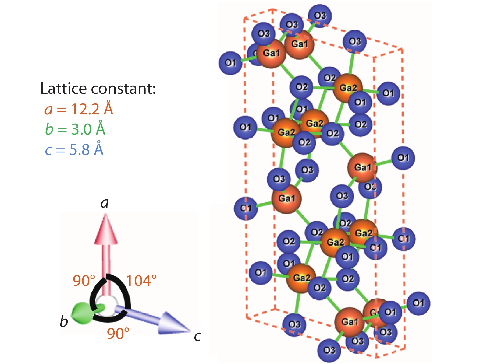
![]()
Figure 1.(Color online) Atomic unit cell of
![]()
Figure 2.Band structure of
3. Bulk substrate growth and thin film epitaxial growth
The success achieving of large diameter single crystalline and low defect density β-Ga2O3 native substrates is the main stimulation of devoting tremendous efforts to realize the application of β-Ga2O3 based materials and devices. Particularly, the development of melt-grown method offers the great promise of accomplishing low cost commercial substrates, which is advantageous over the growth techniques of SiC and bulk GaN. Standard growth techniques of β-Ga2O3 including Czochralski method (CZ)[
![]()
Figure 3.Photograph of 4-inch-diameter
![]()
Figure 4.(Color online)
Developing high quality β-Ga2O3 thin film epitaxial growth is of equal importance when compared to the β-Ga2O3 substrate, since β-Ga2O3 thin film always serve as the channel layer for power devices such as diodes and MOSFETs. Accurate control of the dopants and minimization of defects and imperfections are always two challenges for thin film epitaxial growth. Homoepitaxial growth of high quality β-Ga2O3 thin films on its native substrates can be carried out by the following major ways: metalorganic chemical vapor deposition (MOCVD)[
![]()
Figure 5.(Color online) (a) HRTEM image of an undoped homoepitaxial
4. Device performances: diodes and FETs
As always emphasized by the β-Ga2O3 community, β-Ga2O3 holds promise for future power electronics due to its ultra-wide bandgap, high breakdown field and decent electron mobility induced high BFOM. Table 1 lists the comparisons of some major semiconductors as the channel materials for power devices. Some key FOMs used for representing how ideal of this material can be utilized for power electronics, such as Baliga, Johnson and Keys are also included. Baliga, Baliga high frequency, Johnson and Keyes FOMs are used to evaluate the power devices in terms of power handling capability and conduction loss, the measure of switching losses, the measure of suitability of a semiconductor material for high frequency power transistor applications and requirements, and the thermal dissipation capability for power density and speed, respectively. As shown in this Table 1, all other FOMs of β-Ga2O3 are significantly higher than that of SiC and GaN except Keyes FOM due to its obvious shortage of extremely-low thermal conductivity. Nevertheless, we should put all our endeavors to explore and demonstrate all its potentials and then push the device performance to its limit. Diodes and FETs are the most basic but most important elements of power electronics, which deserve thorough investigation. In this section, the most recent progresses of both diodes and FETs are comprehensively reviewed and solution to its low thermal conductivity issue is proposed.
4.1. Schottky barrier diodes on native substrates
Schottky Barrier Diodes (SBDs) with low turn on voltage (Von), high forward current density and fast switching speed properties are ideal candidate for low switching/conduction losses and high frequency operations, which are indispensible components in power electronic circuits such as converters and inverters for power supplies and power factor corrections[
![]()
Figure 6.(Color online) (a) Electron mobility as a function of carrier concentration. (b)
Following the 1st β-Ga2O3 SBD, many research groups have demonstrated high performance SBDs with BV around or exceeding 1 kV with or without field-plate or edge termination techniques. Konishi et al. reported on the 1st achieving of the BV more than 1 kV with a field-plate structure and a 7-μm thick HVPE grown β-Ga2O3 drift layer[
![]()
Figure 7.(Color online) (a) Forward and (b) reverse
Yang et al. also demonstrated 1 kV-class vertical β-Ga2O3 SBD without field-plate structure with a 10-μm thick β-Ga2O3 drift layer and Ni/Au as the anode[
![]()
Figure 8.(Color online) (a) Reverse
4.2. Field effect transistors (FETs) on native substrates
4.2.1. Depletion-mode high-power FETs
The first metal-semiconductor-FET (MESFET) was demonstrated by Higashiwaki et al. with a Sn-doped β-Ga2O3 epitaxial channel on a semi-insulating (010) β-Ga2O3 substrate[
![]()
Figure 9.(Color online) (a) DC output characteristics of
![]()
Figure 10.(Color online) (a) Schematic cross section of a
![]()
Figure 11.(Color online) (a) Cross-section view and (b) optical image of the fabricated field-plated Ga2O3 MOSFET with SOG S/D doping. (c) Three-terminal breakdown measurement of the field-plated Ga2O3 MOSFET and a record-high BV of 1850 V is demonstrated. Reprinted from IEEE Electron Device Lett, 39, 9 (2018). Copyright of 2018 IEEE[
4.2.2. Enhancement-mode (E-mode) high-power FETs
Zeng et al. reported on achieving the first E-mode β-Ga2O3 MOSFET by adopting a high work function Au gate electrode and low doping (6 × 1015 cm−3) MBE β-Ga2O3 channel, so that E-mode operation with VT of 3 V and BV of 400 V are demonstrated[
![]()
Figure 12.(Color online)
![]()
Figure 13.(Color online) (a) Tilted false-colored SEM image of a fabricated E-mode
![]()
Figure 14.(Color online) (a) Schematic cross-section and (b) SEM image of a vertical E-mode
4.2.3. High frequency RF Power FETs
Green et al. reported on demonstrating the first β-Ga2O3 RF transistor on a Si-doped MOCVD β-Ga2O3 channel with doping concentration of 1018 cm−3 and a (100) substrate[
![]()
Figure 15.(Color online) (a) A device cross section schematic is shown for the
![]()
Figure 16.(Color online) (a) DC output characteristics and pulsed
![]()
Figure 17.(Color online) Transfer characteristics of the thin-channel BGO MOSFET with T-gate. The
4.3. High performance nano-membrane β-Ga2O3 SBDs and FETs on foreign substrates
4.3.1. Field-plated lateral β-Ga2O3 SBDs on sapphire substrate
β-Ga2O3 crystal possesses an unique property that its (100) surface has a large lattice constant of 12.23 Å along [100] direction, which allows a facile cleavage into thin belts or nano-membranes[
![]()
Figure 18.(Color online) (a) Schematic-view and (b) top-view microscopy image of a fabricated lateral
![]()
Figure 19.(Color online) (a) Tilted 3-D schematic-view and (b) top-view microscopy image of a fabricated lateral field-plated
4.3.2. High performance back-gate D/E-modes β-Ga2O3 on insulator (GOOI) FETs
Zhou et al. reported on achieving record-high on-current with a back-gated FETs based on β-Ga2O3 nano-membrane channels[
![]()
Figure 20.(Color online) (a) Schematic view of a GOOI FET with a 300 nm SiO2 layer on Si substrate and (b) AFM image of the atomic flat
![]()
Figure 21.(Color online) (a) and (c) are
4.3.3. VT dependence on the β-Ga2O3 Nano-membrane Thickness
It is found that the VT shifts from negative values in D-mode to positive values in E-mode by shrinking β-Ga2O3 nano-membrane thickness. Fig. 22(a) describes the thickness dependent representative ID–VGS characteristics. Obviously, the VT is shifted from negative to positive when the thickness is slowly reduced. Fig. 22(b) summarizes the extracted thickness dependent VT of 15 devices. Generally, they all follow the same trend as shown in Fig. 22(a). The determined thickness dependent VT may be valuable in the realization of high performance top gate E-mode GOOI FETs in the near future.
![]()
Figure 22.(Color online) (a) Thickness dependent
The significant VT shift with respect to different β-Ga2O3 nano-membrane thickness is due to the surface depletion of the unpassivated device surface, which has tremendous dangling bonds and surface states on the device surface[
![]()
Figure 23.(Color online) (a)
4.3.4. Solutions to the severe self-heating effects on β-Ga2O3 FETs
Self-heating effect induced temperature increase and non-uniform distribution of dissipated power have emerged as one of the most dominant concerns in the degradation of the ID, output power density (P), as well as the gate leakage current, device variability, and reliability[
Figs. 24 (a)–24(c) are the device schematic and SEM images of fabricated GOOI FETs, respectively. Source and drain regions were defined by the VB6 EBL, followed by Ti/Al/Au (15/60/50 nm) metallization and lift-off processes. 15 nm of Al2O3 was deposited by ASM F-120 ALD at 180 °C with tri-methyl-aluminum (TMA) and H2O as precursors. Finally, Ni/Au (50/50 nm) is deposited as the gate electrode, followed with lift-off process.
![]()
Figure 24.(Color online) Cross-section schematic view of a top-gate GOOI FET on (a) SiO2/Si and (b) sapphire and diamond substrates with different κ marked. 15 nm of Al2O3 is used as the gate dielectric, Ti/Al/Au (15/60/50 nm) is used as the source/drain electrodes, and Ni/Au (30/50 nm) is used the gate electrode. (c) False-colored SEM top-view of a GOOI FET with
Figs. 25(a), 25(b) and 25(c) show the well-behaved DC ID–VDS of three top-gate GOOI FETs with LSD of 6/6.5 μm, LG of 1 μm, and channel thickness of 73/75/74 nm on SiO2/Si, sapphire and diamond substrates, respectively. IDMAX of 960, 535 and 325 mA/mm for diamond, sapphire and SiO2/Si substrates are obtained. IDMAX of GOOI FET on diamond and sapphire substrates is around 3 times and 1.7 times of that on SiO2/Si substrate, originating from better transport properties at a lower device temperature. Fig. 25(d) is the ID–VDS comparison at a fixed VGS = 6 V. Figs. 25(e) and 25(f) depict the ID–VGS and gm–VGS of GOOI FETs on three substrates at VDS = 25 V. High on/off ratio of 109 and low SS of 65 mV/dec are achieved on both devices due to the wide bandgap and high-quality ALD Al2O3/β-Ga2O3 interface, yielding a low interface trap density (Dit) of 2.6 × 10¹¹ eV−1·cm−2 by the equation SS = 60 × (1 + qDit/Cox) mV/dec at room temperature, where Cox is the oxide capacitance. One interesting phenomenon is that the peak gm of diamond and sapphire substrate is 34 mS/mm and 21 mS/mm, which is around 2 times and 60% higher than the gm of SiO2/Si substrate. The extrinsic electron field-effect mobility (μFE) of GOOI FET on diamond, sapphire and SiO2/Si are roughly extracted to be 43, 30.2 and 21.7 cm2/(V·s), respectively, benefiting from the less SHE on diamond.
![]()
Figure 25.(Color online)
Figs. 26(a), 26(b) and 26(c) are the merged optical and TR thermal image views of GOOI FETs on SiO2/Si, sapphire and diamond substrates at steady state and different P conditions. As higher VDS is applied, the device is heated up simultaneously and the corresponding ΔT is increased. At P = 717 W/mm2 on the SiO2/Si substrate, the ΔT is measured to be 106 K, whereas in contrast the ΔT is just 43 and 21 K at a higher P = 917 W/mm2 and P = 1237 W/mm2 on the sapphire and diamond substrates, respectively. Fig. 26(d) depicts the measured and simulated ΔT versus P (W/mm2) for the Ga2O3 FETs on a diamond substrate, performed both by TR imaging and Raman thermography. Good agreement among these three methods can be observed, with the highest temperature measured by Raman thermography to be 164 °C (ΔT = 141 K) at DC output power of 6565 W/mm2 (64.7 W/mm or VDS = 35 V for this particular exfoliated FET geometry). Fig. 26(e) shows the good agreement of the TR measured and the simulated ΔT versus P (W/mm2) on different substrates. For both the measurement and simulation results, the clear observation is that at the same P, the GOOI FET on the diamond substrate has more than 8 times lower ΔT compared to that on SiO2/Si. The RT of diamond, sapphire and SiO2/Si substrates are calculated to be 1.71 × 10⁻², 4.62 × 10⁻² and 1.47 × 10⁻¹ mm2·K/W, respectively, through RT = ΔT/P. The reduced RT of GOOI FET on diamond and sapphire demonstrate that a higher κ substrate can be more effective in dissipating the heat on the devices. With less heat on the device, the temperature is lower so that the μ is higher to achieve a higher IDMAX of 960 mA/mm for a better device performance.
![]()
Figure 26.(Color online) TR and charge-coupled device (CCD) camera merged images of GOOI FET on (a) SiO2/Si, (b) sapphire and (c) diamond substrates when device
4.3.5. β-Ga2O3 nano-membrane ferroelectric (FE)-FET with steep ss for wide bandgap logic application
High-temperature solid-state devices and circuits are required for many applications such as in aerospace, automotive, nuclear instrumentations and geothermal wells. Silicon-based complementary metal–oxide–semiconductor (CMOS) technology is not able to operate at such high temperatures, which is limited by its relatively small band gap of 1.12 eV. CMOS circuits using wide band gap semiconductors are promising in these high temperature logic applications. As for the logic application, steep SS is required so as to minimize the power supply so that power consumption and SHE are less severe. In this section, β-Ga2O3 FE-FETs with ferroelectric HZO as a gate dielectric stack is reviewed[
![]()
Figure 27.(Color online) (a) Schematic view of
Fig. 28(a) shows the normalized ID–VGS characteristics in the log scale of a β-Ga2O3 FE-FET. The back-gate bias is swept from −0.4 to 2 V in 40 mV per step, whereas the VDS is biased at 0.1, 0.5, and 0.9 V. The whole sweep takes roughly 1 min. This device has a LCH of 0.5 μm and a thickness of 86 nm. This particular thickness is chosen to tune the VT slightly above zero. The ID−VGS characteristics were measured in bidirectional both forwardly (VGS from low to high) and reversely (VGS from high to low). SS is extracted as a function of ID for both forward sweep (SSmin,For) and reverse sweep (SSmin,Rev) at various VDS. Figs. 28(b)–28(d) show the SS–ID characteristics extracted from Fig. 28(a) at VDS = 0.1, 0.5, and 0.9 V, respectively. The device exhibits SSmin,For = 57.2 mV/dec and SSmin,Rev = 41.0 mV/dec at VDS = 0.1 V, SSmin,For = 53.1 mV/dec and SSmin,Rev = 34.3 mV/dec at VDS = 0.5 V, and SSmin,For = 55.0 mV/dec and SSmin,Rev = 34.4 mV/dec at VDS = 0.9 V. SS less than 60 mV/dec at room temperature is demonstrated for both forward and reverse VGS sweeps even at relatively high VDS. Ga2O3 MOSFETs with 15 nm Al2O3 as a gate dielectric exhibit a minimum SS = 118.8 mV/dec. SS–ID characteristics at different VDS are similar, slightly better at high VDS because of the larger impact of a Schottky barrier at lower VDS. Because of the large band gap of β-Ga2O3, the band-to-band tunneling current at high VDS is suppressed. Fig. 29(a) shows the ID–VGS characteristics in the linear scale of the same β-Ga2O3 FE-FET as in Fig. 28. VT is extracted by linear extrapolation at VDS = 0.1 V for both forward and reverse VGS sweeps. VT in the forward VGS sweep (VT, For) is extracted as 0.47 V, whereas VT in the reverse VGS sweep (VT, Rev) is extracted as 0.38 V. Hence, the E-mode operation with VT greater than zero for both forward and reverse VGS sweeps is demonstrated. A negligible hysteresis is obtained for both on-state (high VGS, as shown in Fig. 10(a)) and off-state (low VGS, as shown in Fig. 28(a)), except that when VGS is near the VT region. At the VT, low hysteresis is achieved to be 90 mV, calculated by using |VT, Rev − VT, For|, showing the great promise of using β-Ga2O3 for wide bandgap logic applications.
![]()
Figure 28.(Color online) (a)
![]()
Figure 29.(Color online) (a)
5. Conclusions
In conclusion, significant progresses have been achieved with remarkable power device performances even at this premature development stage, such as BV more than 3 kV of lateral Schottky Rectifiers, high current density 1.5/1 A/mm of D/E-modes FETs, BV of 1.8 kV for field-plated lateral MOSFET and fT/famx of 5.1/17.1 GHz, respectively. In addition to device performance, sufficient low defect density less than 103 cm−2 of melt-grown native substrate and very smooth surface with RMS roughness less than 0.5 nm of epitaxial β-Ga2O3 thin film on its native substrate have all been demonstrated. However, some open questions about how to realize p-type β-Ga2O3 and how to resolve the low thermal conductivity issue are yet to be established. Once resolving those aforementioned issues, the bright future of β-Ga2O3 devices as power electronic products are definitely coming soon.
References
[1] Y Zhang, i C Joishi, Z Xia et al. Demonstration of
[2] Y Lv, X Zhou, S Long et al. Source-field-plated
[3] A J Green, K Chabak, E R Heller et al. 3.8 MV/cm breakdown strength of MOVPE-grown Sn-doped Ga2O3 MOSFETs. IEEE Electron Device Lett, 37, 902(2016).
[4] K D Chabak, N Moser, A J Green et al. Enhancement-mode Ga2O3 wrap-gate fin field-effect transistors on native (100)
[5] M Tadjer, N Mahadik, V D Wheeler et al. Communications-A (001)
[6] K Zeng, J S Wallace, C Heimburger et al. Ga2O3 MOSFETs using spin-on-glass source/drain doping technology. IEEE Electron Device Lett, 38, 513(2017).
[7] C J H Wort, R S Balmer. Diamond as an electronic material. Mater Today, 11, 22(2008).
[8] H Fu, I Baranowski, X Huang et al. Demonstration of AlN Schottky barrier diodes with blocking voltage over 1 kV. IEEE Electron Device Lett, 38, 1286(2017).
[9] B J Baliga. Power semiconductor-device figure of merit for high-frequency applications. IEEE Electron Device Lett, 10, 455(1989).
[10] H V Wenckstern. Group-III sesquioxides: growth, physical properties and devices. Adv Electron Mater, 3, 1600350(2017).
[11] S Yoshioka, H Hayashi, A Kuwabara et al. Structures and energetics of Ga2O3 polymorphs. J Phys: Condens Matter, 19, 346211(2007).
[12] H He, R Orlando, M A Blanco et al. First-principles study of the structural, electronic, and optical properties of Ga2O3 in its monoclinic and hexagonal phases. Phys Rev B, 74, 195123(2006).
[13] H He, M A Blanco, R Pandey. Electronic and thermodynamic properties of Ga2O3. Appl Phys Lett, 88, 261904(2006).
[14] P Kroll, R Dronskowski, M Martin. Formation of spinel-type gallium oxynitrides: a density-functional study of binary and ternary phases in the system Ga–O–N. J Mater Chem, 15, 3296(2005).
[15] H Y Playford, A C Hannon, E R Barney et al. Structures of uncharacterised polymorphs of gallium oxide from total neutron diffraction. Eur J, 19, 2803(2013).
[16] H Peelaers, C G Van de Walle. Brillouin zone and band structure of
[17] J B Varley, J R Weber, A Janotti et al. Oxygen vacancies and donor impurities in
[18] V I Vasyltsiv, Y I Rym, Y M Zakharo. Optical absorption and photoconductivity at the band edge of
[19] Z Galazka, K Irmscher, R Uecker et al. On the bulk
[20] Z Galazka, R Uecker, K Irmscher et al. Czochralski growth and characterization of
[21] A Kuramata, K Koshi, S Watanabe et al. High-quality
[22] E G Vıllora, Y Morioka, T Atou. Infrared reflectance and electrical conductivity of
[23] J Zhang, B Li, C Xia. Growth and spectral characterization of
[24] N Suzuki, S Ohira, M Tanaka. Fabrication and characterization of transparent conductive Sn-doped
[25] M Mohamed, K Irmscher, C Janowitz et al. Schottky barrier height of Au on the transparent semiconducting oxide
[26] K Suzuki, T Okamoto, M Takata. Crystal growth of
[27] J Zhang, C Xia, Q Deng et al. Growth and characterization of new transparent conductive oxides single crystals
[28] Y Tomm, P Reiche, D Klimm et al. Czochralski grown Ga2O3 crystals. J Cryst Growth, 220, 510(2000).
[29] Z Galazka, R Uecker, D Klimm et al. Scaling-up of bulk
[30] M Higashiwaki, A Kuramata, H Murakami et al. State-of-the-art technologies of gallium oxide power devices. J Phys D, 50, 333002(2017).
[31] K Hoshikawa, E Ohba, E Kobayashi et al. Growth of
[32] F Alema, B Hertog, A Osinsky et al. Fast growth rate of epitaxial
[33] D Gogova, G Wagner, M Baldini et al. Structural properties of Si-doped
[34] M Baldini, M Albrecht, A Fiedler et al. Semiconducting Sn-doped
[35] K Sasaki, M Higashiwaki, A Kuramata et al. Growth temperature dependences of structural and electrical properties of Ga2O3 epitaxial films grown on
[36] T Oshima, T Okuno, S Fujita. Ga2O3 thin film growth on
[37] H Okumura, M Kita, K Sasaki et al. Systematic investigation of the growth rate of
[38] T Oshima, N Arai, N Suzuki et al. Surface morphology of homoepitaxial
[39] Y Oshima, E G Vıllora, K Shimamura. Halide vapor phase epitaxy of twin-free α-Ga2O3 on sapphire (0001) substrates. Appl Phys Express, 8, 055501(2015).
[40] T Watahiki, Y Yuda, A Furukawa et al. Heterojunction p-Cu2O/n-Ga2O3 diode with high breakdown voltage. Appl Phys Lett, 111, 222104(2017).
[41] H Murakami, K Nomura, K Goto et al. Homoepitaxial growth of
[42] K Nomura, K Goto, i R Togashi et al. Thermodynamic study of
[43] C Hebert, A Petitmangin, J Perrie're et al. Phase separation in oxygen deficient gallium oxide films grown by pulsed-laser deposition. Mater Chem Phys, 133, 135(2012).
[44] Z Chen, X Wang, S Noda et al. Effects of dopant contents on structural, morphological and optical properties of Er doped Ga2O3 films. Superlattices Microstruct, 90, 207(2016).
[45] T Kawaharamura. Physics on development of open-air atmospheric pressure thin film fabrication technique using mist droplets: Control of precursor flow. Jpn J Appl Phys, 53, 05F(2014).
[46] S D Lee, K Kaneko, S Fujita. Homoepitaxial growth of beta gallium oxide films by mist chemical vapor deposition. Jpn J Appl Phys, 55, 1202B(2016).
[47] G T Dang, T Kawaharamura, M Furuta et al. Metal–semiconductor field-effect transistors with In–Ga–Zn–O channel grown by nonvacuum-processed mist chemical vapor deposition. IEEE Electron Device Lett, 36, 463(2015).
[48] S Fujita, K Kaneko. Epitaxial growth of corundum-structured wide band gap III-oxide semiconductor thin films. J Cryst Growth, 401, 588(2014).
[49] K Akaiwa, S Fujita. Electrical conductive corundum-structured α-Ga2O3 thin films on sapphire with tin-doping grown by spray-assisted mist chemical vapor deposition. Jpn J Appl Phys, 51, 070203(2012).
[50] M Baldini, M Albrecht, D Gogova et al. Effect of indium as a surfactant in (Ga1−
[51] Z Hu, H Zhou, Q Feng. Field-plated lateral
[52] K Sasaki, A Kuramata, T Masui et al. Device-quality beta-Ga2O3 epitaxial films fabricated by ozone molecular beam epitaxy. Appl Phys Exp, 5, 035502(2012).
[53] K Konishi, K Goto, H Murakami et al. 1-kV vertical
[54] J Yang, S Ahn, F Ren et al. High reverse breakdown voltage Schottky rectifiers without edge termination on
[55] J Yang, S Ahn, F Ren et al. High breakdown voltage (−201)
[56] J Yang, F Ren, S J Pearton et al. Vertical geometry 2-A forward current Ga2O3 Schottky rectifiers on bulk Ga2O3 substrates. IEEE Trans Electron Devices, 65, 2790(2018).
[57] M Higashiwaki, K Sasaki, A Kuramata et al. Gallium oxide (Ga2O3) metal−semiconductor field-effect transistors on single-crystal
[58] M H Wong, K Sasaki, A Kuramata et al. Field-plated Ga2O3 MOSFETs with a breakdown voltage of over 750 V. IEEE Electron Device Lett, 37, 212(2016).
[59] K Zeng, A Vaidya, U Singisetti et al. 1.85 kV breakdown voltage in lateral field-plated Ga2O3 MOSFETs. IEEE Electron Device Lett, 39, 1385(2018).
[60]
[61] Z Hu, K Nomoto, W Li et al. Enhancement-mode Ga2O3 vertical transistors with breakdown voltage >1 kV. IEEE Electron Device Lett, 39, 869(2018).
[62] A J Green, K D Chabak, M Baldini et al.
[63] M Singh, M A Casbon, M J Uren et al. Pulsed large signal rf performance of field-plated Ga2O3 MOSFETs. IEEE Electron Device Lett, 39, 1572(2018).
[64]
[65] W S Hwang, A Verma, H Peelaers et al. High-voltage field effect transistors with wide-bandgap beta-Ga2O3 nanomembranes. Appl Phys Lett, 104, 203111(2014).
[66] Z Hu, H Zhou, K Dang et al. lateral-Ga2O3 schottky barrier diode on sapphire substrate with reverse blocking voltage of 1.7 kV. IEEE J Electron Device Soc, 6, 815(2018).
[67] H Zhou, K Maize, G Qiu et al.
[68] H Zhou, M Si, S Alghamdi et al. High performance depletion/ enhancement mode
[69] N A Moser, J P Mccandless, A Crespo et al. High pulsed density
[70] S H Shin, M A Wahab, A Masuduzzaman et al. Direct observation of self-heating in III–V gate-all-around nanowire MOSFETs. IEEE Trans Electron Devices, 62, 3516(2014).
[71] H Zhou, K Maize, J Noh et al. Thermo-dynamic studies of
[72] J Noh, M Si, H Zhou et al. The impact of substrates on the performance of top-gate
[73] K Maize, A Zibari, W D French et al. Thermoreflectance CCD imaging of self-heating in power MOSFET arrays. IEEE Trans Electron Devices, 61, 3047(2014).
[74] M Si, L Yang, H Zhou et al.

Set citation alerts for the article
Please enter your email address
© Copyright 2018-2021 | Chinese Laser Press. All Rights Reserved 沪ICP备15018463号-20