
Zhiting Lin, Zhongzhen Tong, Jin Zhang, Fangming Wang, Tian Xu, Yue Zhao, Xiulong Wu, Chunyu Peng, Wenjuan Lu, Qiang Zhao, Junning Chen. A review on SRAM-based computing in-memory: Circuits, functions, and applications[J]. Journal of Semiconductors, 2022, 43(3): 031401
- Journal of Semiconductors
- Vol. 43, Issue 3, 031401 (2022)
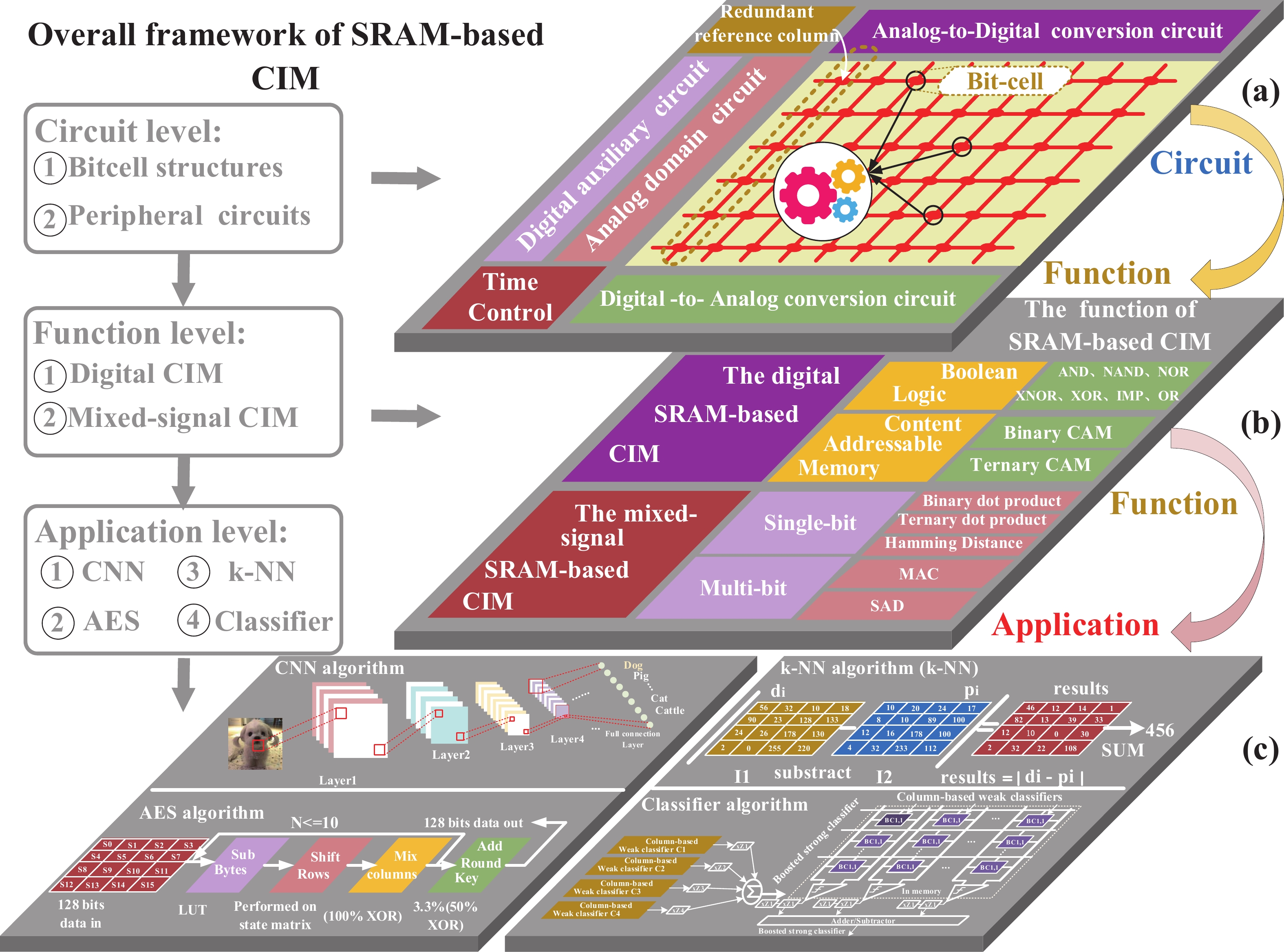
Fig. 1. (Color online) Overall framework of static random-access memory (SRAM)-based computing in-memory (CIM) for the review: (a) various functions implemented in CIM, (b) operation functions realizable with CIM, and (c) application scenarios of CIM.
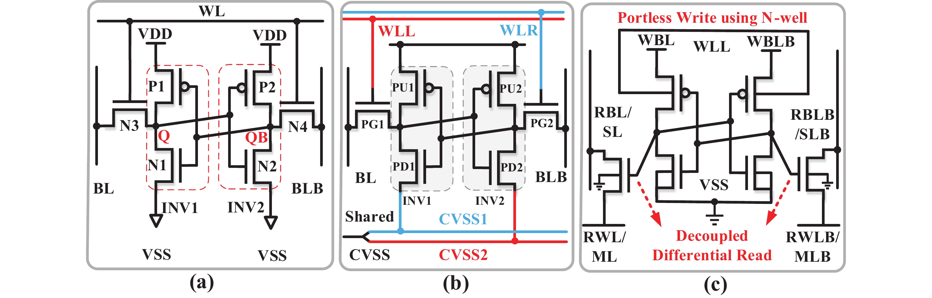
Fig. 2. (Color online) (a) Standard 6T SRAM cell, (b) dual-Split 6T SRAM cell, and (c) 4+2T SRAM cell.
Fig. 3. (Color online) SRAM cells with separated read and write: (a) standard 8T SRAM bit-cell, (b) 7T SRAM cell, (c) 9T SRAM cell, and (d) 10T SRAM cell.
Fig. 4. (Color online) SRAM cells based on capacitive coupling: (a) C3SRAM bitcell and (b) M-BC bitcell.
Fig. 5. (Color online) (a) Transposable bitcell contains two pairs of access transistors and (b) separated read–write transposable bit cell. (c) Schematic of the transposable 10T bit bitcell.
Fig. 6. (Color online) Compact coupling structure: (a) 12T cell and (b) two-way transpose multibitcell.
Fig. 7. (Color online) (a) Asymmetric differential sense amplifier (SA), (b) flash ADC, and (c) successive approximation ADC.
Fig. 8. (Color online) (a) Weighted array with different capacitor sizes and (b) multi-period weighting technique using capacitors of the same size.
Fig. 9. (Color online) Schematic of the column-wise GBL_DAC circuit: (a) Circuit of the constant current source, (b) two-stage MUX, and (c) waveform of the column-wise GBL_DAC circuit. (d) Schematic and waveform of the pulse height modulation circuit.
Fig. 10. (Color online) Redundant reference column technology.
Fig. 11. (Color online) (a) In-/near-memory computing peripherals and (b) a bit-tree adder.
Fig. 12. (Color online) Signed 4-b × 8-b least significant bit (LSB) multiplier: (a) timing diagram and (b) circuit schematic.
Fig. 13. (Color online) Boolean operation: (a) Boolean logical operations using an SRAM array, (b) histogram of AND and NOR operation voltages, and (c) schematic of the 8T-SRAM for implementing the IMP and XOR operations.
Fig. 14. (Color online) Column-wise BCAM: (a) search example in 3D-CAM and (b) 4+2T. Row-wise TCAM: (c) organization based on 10T and (d) organization based on 6T.
Fig. 15. (Color online) Schematic and truth table of the binary dot product: (a) 6T-SRAM binary dot product and (b) 8T-SRAM binary dot product. (c) Ternary dot product: operation of ternary multiplication and XNOR value mapping table.
Fig. 16. (Color online) Row of 9T SRAM cells for calculating the Hamming distance.
Fig. 17. (Color online) (a) Precharge weighting technology, (b) pulse width weighting, (c) pulse height weighting, and (d) pulse number weighting.
Fig. 18. (Color online) (a) 8T-SRAM memory array for computing dot products with 4-bit weight precision and (b) Twin-8T cell.
Fig. 19. (Color online) (a) Schematic of SAD circuit and (b) sequence diagram.
Fig. 20. (Color online) Implementation of (a) CNN and (b) AES on multiple SRAM arrays.
Fig. 21. (Color online) Application in the k-NN algorithm.
Fig. 22. (Color online) Application in classifier algorithms.
Fig. 23. (Color online) Read disturb issue.
Fig. 24. (Color online) (a) Single row activation during normal SRAM read operation, (b) multirow read and nonlinearity during CIM, and (c) inconsistent CIM calculation.
Fig. 25. (Color online) Approach of mapping from the common operator set to the actual circuits.
Fig. 26. (Color online) Architecture of the bidirectional CIM system, including a reusable and reconfigurable module.
Fig. 27. (Color online) Multithreaded CIM macro based on a pipeline processor.
| ||||||||||||||||||||||||||||||||||||||||||||||||||||||||||||||||||||||||||||||||||||||||||||||||||||||||||||||||||||||||||||||||||||||||||||||||||||||||||||||||||||||||||||
Table 1. Static random-access memory (SRAM) bitcells in CIM.
| |||||||||||||||||||||||||||||||||||||||||||||||||||||||||||||||||||||||||||||||||||||||||||||||||||||||||||||||||||||||||||||
Table 2. Summary of chip parameters and performance of in-memory Boolean logic and CAM
| |||||||||||||||||||||||||||||||||||||||||||||||||||||||||||||||||||||||||||||||||||||||||||||||||||||||||||||||||||||||||||||||||||||||||||||||||||||||||
Table 3. Summary of chip parameters and performance of single- and multibit operations.


Set citation alerts for the article
Please enter your email address

© Copyright 2018-2021 | Chinese Laser Press. All Rights Reserved 沪ICP备15018463号-20