
Zhiting Lin, Zhongzhen Tong, Jin Zhang, Fangming Wang, Tian Xu, Yue Zhao, Xiulong Wu, Chunyu Peng, Wenjuan Lu, Qiang Zhao, Junning Chen. A review on SRAM-based computing in-memory: Circuits, functions, and applications[J]. Journal of Semiconductors, 2022, 43(3): 031401
- Journal of Semiconductors
- Vol. 43, Issue 3, 031401 (2022)
Abstract
1. Introduction
Recently, with the breakthrough of key technologies such as big data and artificial intelligence (AI), emerging intelligent applications represented by edge computing and intelligent life have emerged in the trend of the era of rapid development[
As a computing paradigm that may address the von Neumann bottleneck, researchers have proposed the computing in-memory (CIM) technology. The so-called CIM is a new architecture and technology for computing directly in memory. It breaks through the limitation of traditional architecture, optimizes the structure of storage unit and logic unit, realizes the integration of storage unit and logic unit, and avoids the cumbersome process of transmitting data to processor register for calculation and then back to memory, thus significantly reducing the delay and energy consumption of the chip[
To improve the performance of the SRAM-based CIM, the SRAM bitcell structure has been modified and auxiliary peripheral circuits have been developed. For example, read–write isolation 8T[
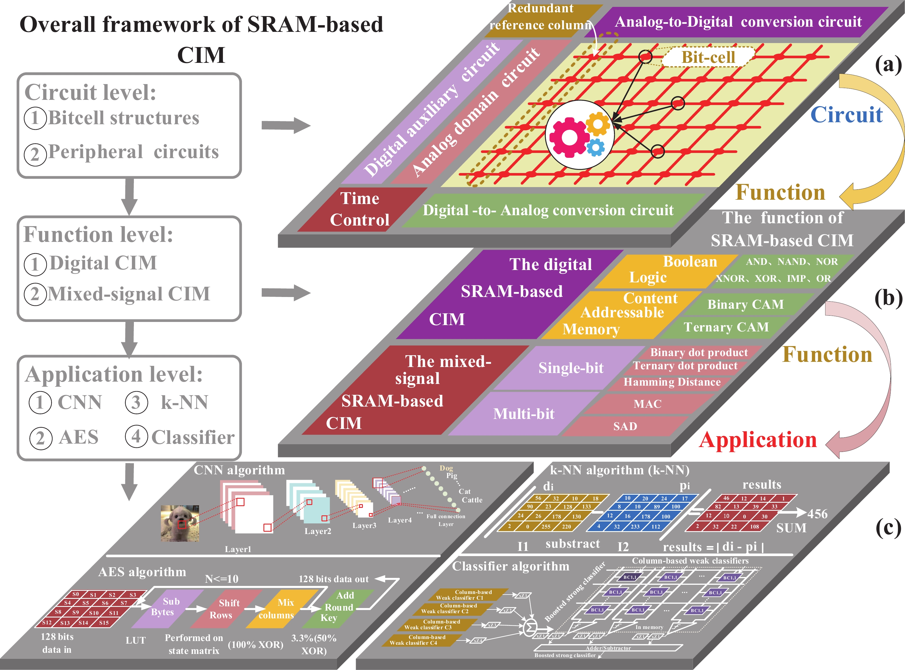
As illustrated in Fig. 1, we reviewed three levels of SRAM-based CIM: circuit, function, and application. The circuit level is reviewed from two aspects: 1) bitcell structures, which include read–write separation structures, transposable structures, and compact coupling structures, and 2) peripheral auxiliary circuits, which include analog-to-digital conversion circuits, digital-to-analog conversion circuits, redundant reference columns, digital auxiliary circuits, and analog auxiliary circuits (Fig. 1(a)). The second level is reviewed from two aspects: 1) pure digital CIM, which includes Boolean logic and CAM, and 2) mixed-signal CIM functions, which include MAC, Hamming distance, and SAD (Fig. 1(b)). The third level is mainly reviewed from the aspects of the application of the accelerating CNN, classifier, k-NN, and AES algorithms (Fig. 1(c)). Finally, the challenges and future development prospects of SRAM-based CIM are discussed from these three levels.
![]()
Figure 1.(Color online) Overall framework of static random-access memory (SRAM)-based computing in-memory (CIM) for the review: (a) various functions implemented in CIM, (b) operation functions realizable with CIM, and (c) application scenarios of CIM.
2. Memory cell in static random-access memory (SRAM)-based computing in-memory (CIM)
In the core module of the SRAM, the memory cell occupies most of the SRAM area. Irrespective of the complexity of operations implemented in the memory unit, the primary challenge is to fully leverage the memory cells. In this section, we analyze and summarize the cell structures in the SRAM-based CIM. Additionally, we compare the performances of the reconstructed SRAM cell and the traditional structure and discuss the possible research direction of CIM in terms of the cell structure.
2.1. Structure of the 6T cell
2.1.1. Standard 6T-SRAM structure
Standard 6T structures have been adopted in most system-on-chips (SoCs) for their high robustness and access speed. Previous studies on CIM, including Refs. [15, 16, 19, 20, 24-26, 29, 33, 35, 39-53] and Ref. [34], used standard 6T cells considering the area overhead. Fig. 2(a) illustrates a schematic of the standard 6T SRAM cell. The 6T storage cell is composed of two P-channel metal–oxide–semiconductors (PMOSs) and four N-channel metal–oxide–semiconductors (NMOSs), in which P1, N1, P2, and N2 constitute two cross-coupled inverters to store data stably. To perform CIM with the conventional 6T SRAM cell, the operands are commonly represented by the word line (WL) voltage and storage node data. The processing results are often reflected by the voltage difference between BL and BLB.
![]()
Figure 3.(Color online) SRAM cells with separated read and write: (a) standard 8T SRAM bit-cell, (b) 7T SRAM cell, (c) 9T SRAM cell, and (d) 10T SRAM cell.
2.1.2. Dual-split 6T cell
Khwa et al.[
2.1.3. 4+2T SRAM cell
Dong et al.[
2.2. Cell structure with additional devices for SRAM-based CIM
The simple 6T structure cannot realize complex computing operations and does not fully meet the requirements of CIM. Therefore, studies on CIM have modified the traditional 6T structure, which can be roughly divided into the following four categories.
2.2.1. SRAM cells with separated read and write paths
Compared with the 6T cell, SRAM cells with separated read and write do not suffer from reading–writing disturbances; hence, within the memory array, it can simultaneously activate multiple read WLs to complete the operation. These cells contain a standard 6T cell and an additional read port composed of extra transistors to separate read and write. The write operation is similar to that of a traditional 6T cell. For the read operation, these cells can read data through a read bit line (RBL) discharge or charge.
Fig. 3(a) presents a schematic of a standard 8T cell, where M2 and M1 form an additional read port. A large number of pioneering works have used standard 8T cells to complete CIM operations, including a multibit dot-product engine for computing acceleration[
![]()
Figure 2.(Color online) (a) Standard 6T SRAM cell, (b) dual-Split 6T SRAM cell, and (c) 4+2T SRAM cell.
2.2.2. SRAM cells based on capacitive coupling
SRAM cells based on capacitive coupling add additional capacitances inside the cell to perform the operations. Jiang et al.[
![]()
Figure 4.(Color online) SRAM cells based on capacitive coupling: (a) C3SRAM bitcell and (b) M-BC bitcell.
In Refs. [31, 58], the capacitance in the cell can be directly coupled and shared through the MBL. However, in Refs. [59, 60], the capacitors inside the unit need to be coupled with each other through additional switches. Therefore, in the latter work, additional transistors need to be introduced, which increases the area of the cell. In the selection of capacitance type, Refs. [31, 58] selected MOSCAP which constitutes 27% of the bitcell area. However, Refs. [59, 60] selected MOMCAP that is formed using metal-fringing structures. MOMCAP can be placed on the top of the cell, so there is no additional area overhead. However, compared with MOSCAP, MOMCAP has a lower capacitance density and is not suitable for large capacitances.
2.2.3. Transposable SRAM cell
Fig. 5 presents three different forms of transposable bitcells: 1) Wang et al.[
![]()
Figure 2.(Color online) (a) Standard 6T SRAM cell, (b) dual-Split 6T SRAM cell, and (c) 4+2T SRAM cell.
2.2.4. Compact coupling structure
The basic reading and writing operations of the compact-coupling structure are consistent with traditional SRAM. However, exclusive and independent structures have been developed for CIM operations. Yin et al.[
![]()
Figure 8.(Color online) (a) Weighted array with different capacitor sizes and (b) multi-period weighting technique using capacitors of the same size.
Both structures are based on traditional 6T cells, which perform operations by adding compact-coupled computing units. This strategy can maintain the basic read and write capabilities of SRAM while allowing it to perform complex operations. However, the compact-coupling module also increases the area overhead and complexity of the peripheral control circuit.
Table 1 summarizes various types of SRAM-based CIM bitcell. It was found that the area efficiency of the previous study was related to the structure of the basic cells. In CIM, two main approaches are used to design the bitcell: 1) maintaining the standard 6T and 2) reconstructing basic units by adding additional transistors or capacitors. Currently, the main purpose of cell design in CIM is to realize novel operations, and the automatic restoration of operation results is not realized. In the future, the unit design will focus on the processing of operation results.
3. Peripheral auxiliary circuits of the SRAM-based CIM
Depending on the basic cells in the array, only limited digital computing functions can be achieved. Peripheral circuits, such as high-precision ADC, weight processing, generation of reference voltage, pulse modulation, and near memory multiplication, must be used with the SRAM system to achieve high-performance memory operations or analog domain computation.
3.1. Analog-to-digital conversion (ADC) circuit
An ADC circuit is indispensable in processing computational results in an array (mostly analog value represented by the BL voltage). It has two main roles: 1) quantifying the BL voltage and 2) weighting the BL voltage.
3.1.1. Quantifying BL voltage
As shown in Fig. 7(a), it is an asymmetrically sized sense amplifier (SA)[
![]()
Figure 9.(Color online) Schematic of the column-wise GBL_DAC circuit: (a) Circuit of the constant current source, (b) two-stage MUX, and (c) waveform of the column-wise GBL_DAC circuit. (d) Schematic and waveform of the pulse height modulation circuit.
Sinangil et al.[
In Ref. [32], Si et al. used several capacitors with different values to generate different reference voltages to quantify the analog voltage of the RBL. RBL shares its charge with the capacitor array after multicycle operations (Fig. 7(c)). In this design, capacitors with different values are sequentially connected to one of the two ends of the SA through a switch; that is, a stepwise comparison is performed through multiple operation stages to quantify the analog voltage of the RBL.
The quantifying circuits process the final calculation result, which is especially important for the calculation accuracy of the entire system. Most researchers choose flash ADC[
3.1.2. Weighting BL voltage circuits
One of the weighting BL voltage circuits is the capacitor array weighting circuits. It has a higher linearity, which is often used when high-precision operations are required. Capacitor array weighting techniques are broadly grouped into two categories:
1) Weighting by different capacitor sizes[
![]()
Figure 10.(Color online) Redundant reference column technology.
2) Weighting by sharing charge across multiperiod operations, as shown in Fig. 8(b). In Ref. [64], the parasitic capacitance on the BL was the same as that of C_DIV in the capacitor array, so that the charge was shared equally among the capacitors. When 1/8 weighting was required, in the first period, the BL was connected to port 2 achieving the charge sharing with three C_DIVs. Thus, the voltage decreased to 1/4. In the second period, the BL was connected to port 1, and the shared charge was divided equally. Therefore, the original charge was ultimately divided into 1/8 of the original charge. Charge can be shared in multiperiod operations in a similar manner to achieve other weights.
The two types of weighting techniques have their demerits. In the first technique, the capacitance increases exponentially with the number of input bits, which increases the area overhead exponentially. However, in that work its unit of computation capacitance is formed by the inherent cap of the sense amplifier (SA) inside the 4-bit Flash ADC, which saves area and minimizes the kick-back effect. Moreover, it is difficult to realize in the manufacturing process. In the second technique, the capacitance of the circuit remains unchanged. However, multiple operation periods are required to complete the weighting, which decreases the computation speed. In general, whether it is the equivalent capacitance of SA, MOMCAP or MOSCAP, if there has a large capacitance in the CIM system, the robustness of the operations will have a certain impact.
3.2. Digital-to-analog (DAC) conversion circuit
The purpose of the DAC circuit is to convert a digital input into the corresponding analog quantity as the pulse width or pulse height. The BL voltage can be decreased or increased proportionately by controlling the pulse width or pulse height in proportion to the digital input. The precise generation of these widths or heights is crucial to multibit calculation.
For example, for an input of 6 bits, the circuit design requires 64 different pulse widths. Generating such a variety of pulse widths in the memory consumes an immense area and power. Therefore, the solution to this problem requires a delicate circuit. Biswas et al.[
![]()
Figure 1.(Color online) Overall framework of static random-access memory (SRAM)-based computing in-memory (CIM) for the review: (a) various functions implemented in CIM, (b) operation functions realizable with CIM, and (c) application scenarios of CIM.
As shown in Fig. 9(d), the DAC circuit, used for pulse height modulation, is composed of a binary weight current source and a copy unit[
The DAC precisely controls the proportional discharge of transistors. However, the transistor itself is a nonlinear device, so the discharge rate cannot be controlled proportionally. Thus, both techniques encounter the problem of nonlinear calculation results. Solving this is particularly important for the SRAM-based CIM.
3.3. Redundant reference column circuit
The in-memory Boolean logic, CAM operation, and MAC require multiple reference voltages. In practice, multiple reference voltages cannot be simultaneously connected due to the limited external pins of the chip. To address this, multiple reference voltages must be implemented in an array. A common technique for generating the required reference voltages in an array is by the redundant reference column circuit.
As shown in the orange rectangle in Fig. 10[
![]()
Figure 3.(Color online) SRAM cells with separated read and write: (a) standard 8T SRAM bit-cell, (b) 7T SRAM cell, (c) 9T SRAM cell, and (d) 10T SRAM cell.
3.4. Digital auxiliary computing circuit
Although most of the repeated operation functions are completed in the analog domain, the accumulation of the analog results is technically difficult. Digital domain accumulation is a good choice, and digital auxiliary circuits can significantly improve the computational accuracy of the system.
Fig. 11(a) illustrates a digital-aided technique for 2- and 3-bit multiplication. The Boolean logic “AND” and “NOR” functions are realized by an SA sensing the voltage of column CBL or CBLB[
![]()
Figure 5.(Color online) (a) Transposable bitcell contains two pairs of access transistors and (b) separated read–write transposable bit cell. (c) Schematic of the transposable 10T bit bitcell.
The digital circuit not only assists in the execution of multiplication but also the MAC, as shown in Fig. 11(b)[
Digital calculations are highly precise. However, this method requires multiple cycles and has a relatively large area overhead and power consumption. The efficient use of digital circuits is a research direction in in-memory computing.
3.5. Analog auxiliary computing circuit
The analog domain auxiliary circuit has a lower calculation accuracy than its digital counterpart; however, it can achieve a higher computing ability with limited area and energy consumption. Kang etal.[
![]()
Figure 6.(Color online) Compact coupling structure: (a) 12T cell and (b) two-way transpose multibitcell.
4. Computational functions of the SRAM-based CIM
Because the internal cells of an SRAM array are repetitive, the operation in memory must be simple and repeatable. The existing SRAM-based CIM can be classified into two: pure digital CIM and mixed-signal CIM. The pure digital CIM mainly includes Boolean operation and CAM, and the mixed-signal CIM the processing of the Hamming distance, MAC, and SAD.
4.1. Digital SRAM-based CIM
4.1.1. Boolean logic (AND, OR, NAND, NOR, XNOR, XOR, and IMP)
Implementing the Boolean logic in memory is relatively simple and accurate because its operation is completed in the digital domain. Fig. 13(a) illustrates a basic construct for performing in-place bitwise logical operations using SRAM[
![]()
Figure 7.(Color online) (a) Asymmetric differential sense amplifier (SA), (b) flash ADC, and (c) successive approximation ADC.
Most of the existing Boolean logics are realized by opening two rows of cells and sensing the BL voltage by setting the SA reference voltage[
4.1.2. Content addressable memory (CAM)
The CAM is a special type of memory that can automatically compare input data with all the data stored in the array simultaneously to determine whether the input data matches the data in the array. The realization of CAM in SRAM can reduce data transmission and avoid a large amount of energy consumption. The CAM operation can be divided into binary CAM (BCAM) and fault-tolerant ternary CAM (TCAM). In addition, there are two different search modes, including row-wise search and column-wise search. The row-wise search is defined as the cases where the input searching data are represented by lines connected by rows. Similarly, the column-wise search is defined as the cases where the input searching data are represented by lines connected by columns. In Figs. 14, (a) and (b) are the column-wise BCAM operations, and (c) and (d) are the row-wise TCAM operations. Srinivasa et al.[
![]()
Figure 8.(Color online) (a) Weighted array with different capacitor sizes and (b) multi-period weighting technique using capacitors of the same size.
The difference between TCAM and BCAM is that the former has a do-not-care state. Two cells are used to represent one data point owing to the presence of three states in the TCAM. The three states, 0/1/X (where X is an independent state, a do-not-care state), are represented by 00/11/01, respectively, whose implementation for column-wise search is shown in Fig. 14(c). The data to be searched is represented by two adjacent cells in a row, and the search data by the SL/SLB voltage. The intermediate ML1’/ML2 of two adjacent columns are shielded, and the matching result is determined by whether the other two MLs are discharged[
Lin et al.[
In Table 2, the performances of several CIM Boolean logics and CAM are compared and the different search modes are presented. Most studies have implemented both Boolean operations and CAM by modifying standard cells, indicating the compatibility of these two functions. However, few have achieved CAM function in two directions simultaneously. Currently, in-memory Boolean logic is realized at the cost of reduced parallelism as opposed to its analog counterpart. Therefore, improving the parallelism for Boolean logic and using it to achieve sophisticated calculations in memory will be a direction for research.
4.2. Mixed-signal SRAM-based CIM
The mixed-signal SRAM-based CIM is primarily categorized into two types: 1) single-bit operation, including binary and ternary dot products, and Hamming distance, and 2) multibit operation, including multibit multiplication and SAD.
4.2.1. Single-bit operation0
A. Binary dot product
The multiplication operation of a single bit is also a dot-product operation. As mentioned previously, there are two subtypes of this operation: binary and ternary dot products. Chiu et al. executed (1,0) × (1,0) and (1,0) × (+1, -1) dot-product operations with standard 6T cells[
![]()
Figure 11.(Color online) (a) In-/near-memory computing peripherals and (b) a bit-tree adder.
The cumulative result of the above study is on the BL; therefore, the operation should be performed by columns. However, in the traditional SRAM storage mode, data are stored row-wise. The CIM mode conflicts with the storage mode, which reduces the operation efficiency. To address this problem, Agrawal et al. used a 10T SRAM to perform a binary line dot product, and the results were reflected on the horizontal source lines[
B. Ternary dot product
Yin et al. achieved a ternary dot product[
As the input and weight of the dot-product operation are in single bits, no additional auxiliary circuits are required to process the weight, and the quantization of the operation results is simplified. The dot-product operation can be applied to the binary neural network (BNN) algorithm, where the inputs can be restricted to either +1/–1 or 0/1. When the inputs are restricted to 0 or 1, it has a 0.03% loss of accuracy compared with +1/–1 input, which is tested in the MNIST dataset[
C. Hamming distance
The Hamming distance algorithm is widely used in signal processing and pattern recognition. The Hamming distance between any two vectors of the same length is defined as the number of corresponding bits with different values. The principle of Hamming distance is that two bytes of the same length are bitwise XNOR and these XNOR results are then accumulated. For example, the Hamming distance from 1101 to 0111 is 2. Because this algorithm also requires high data access, it consumes a significant amount of energy when used in the traditional architecture.
Ali et al. proposed a 9T SRAM to calculate the Hamming distance[
![]()
Figure 13.(Color online) Boolean operation: (a) Boolean logical operations using an SRAM array, (b) histogram of AND and NOR operation voltages, and (c) schematic of the 8T-SRAM for implementing the IMP and XOR operations.
Unlike the row-wise Hamming distance operations, Kang et al. proposed a column-wise Hamming-distance macro based on a 6T SRAM array[
In CIM, most of the results are reflected on BLs of column-wise connection. Therefore, vertical data storage is generally required, increasing the implementation complexity for the SRAM writing mode. For example, Jeloka et al. proposed a strategy of column-wise write[
4.2.2. Multibit operation
Unlike single-bit operations wherein the operands are limited to only 0, –1, and 1, multibit operations can obtain more precise in-memory computations, which meets the requirements of various AI algorithms. There are two main categories of multibit operations: 1) multibit multiplication and 2) SAD.
A. Multibit multiplication
The key to multibit multiplication is the weighting strategy. The weighting strategies include pulse width[
1) Precharge time weighting
Fig. 17 illustrates various pulse-based weighting techniques. Ali et al.[
![]()
Figure 16.(Color online) Row of 9T SRAM cells for calculating the Hamming distance.
2) Pulse-width-weighting
During the SRAM read operation, when the BL voltage is maintained within a certain range, its discharge voltage is proportional to the WL turn-on time; that is, the decrease of the BL voltage can be controlled by controlling the opening time of the WL. Therefore, by doubling the opening width of each WL, a proportional increase in the BL voltage change can be obtained. Sujan et al.[
3) Pulse height weighting
As shown in Fig. 17(c), different pulse heights can be applied to the WL or BL. Zhang et al.[
4) Weighting strategy based on the number of pulses
Dong et al.[
5) Weighting strategy based on the transistor width–length ratio
As depicted in Fig. 18(a), in the 8T array, the sizes of the read access transistors in different columns are adjusted in proportion to the weights of the input data[
![]()
Figure 19.(Color online) (a) Schematic of SAD circuit and (b) sequence diagram.
Different designs have tradeoffs among time cost, implementation difficulty, linearity, area cost, and process. 1) Precharge time weighting: When the precharge and the word line are turned on simultaneously, there will be a relatively large current which will increase power consumption. 2) Pulse-width-weighting: Its operation is relatively simple. However, when the input bits increase, the corresponding pulse width will increase proportionally; thus, the time increases exponentially, resulting in a significant decrease in calculation speed. Moreover, when the bit line voltage is relatively low, linearity will also be a problem. 3) Pulse height weighting: The V–I characteristic of metal–oxide–semiconductor (MOS) devices is that the current between the source and drain increases proportionally to the square of the gate voltage. Therefore, unlike 2), the pulse height cannot be increased proportionally to ensure proportional discharge of the bit line, so it is difficult to set the pulse height. In addition, the linearity is relatively poor compared with 2). 4) Pulse number weighting: As this design controls the discharge numbers of the access transistor, it is basically consistent with 2); thus, there will be similar problems. 5) Weighting based /on transistor width–length ratio: The proportional discharge of bit line can be realized by adjusting the width–length ratio of transistors. However, increasing the size of the transistor will also increase the area overhead, bring difficulties to the layout process and cause mismatch due to the oversized array ratio. The above weighting design methods are all a tradeoff between the octagonal rules of circuit design.
B. Sum of absolute difference (SAD)
To implement the SAD, we must first obtain the absolute difference (AD),
where
Kang et al. executed a SAD operation based on a 6T SRAM array without sacrificing storage density[
![]()
Figure 2.(Color online) (a) Standard 6T SRAM cell, (b) dual-Split 6T SRAM cell, and (c) 4+2T SRAM cell.
Table 3 summarizes the performances of existing single and multibit operations. The number of input and output bits reflect the performance of the operation. However, the difficulty lies in improving the effective number of bits (ENOB) of the final output result without using a high ENOB ADC. This is because the overhead of a high ENOB ADC is unacceptable as it deviates from the original intention of low-overhead in-memory computing.
5. Application scenarios for CIM
The computing functions realizable by CIM have been widely used in various fields, including image and voice recognition, which require data exchange between encryption and decryption algorithms for data security. In this section, the application scenarios of CIM, including CNN, AES, k-NN, and classifier algorithms, are introduced.
5.1. Application in CNNs
Inspired by biological neural networks, artificial neural networks are used in image processing and speech recognition. A deep neural network (DNN) contains at least two layers of nonlinear neural units connected via adjustable synaptic weights. These weights can be updated according to the input data to optimize the output. In 1990, a dedicated hybrid chip was developed for multilayer neural networks[
CNN algorithms evolved from DNN algorithms are fully applied in image processing. A CNN algorithm can be mapped onto multiple intercommunicating SRAM arrays, as illustrated in Fig. 20(a). Each layer of the CNN contains several repetitive MAC operations, and implementing these MACs in the traditional von Neumann architecture results in a large overhead. In CIM, the weights of the layer are stored in SRAM cells, and the input is represented by WLs or BLs. A large amount of data flowing between the processor and the memory is eliminated. The final accumulation results are often reflected in the BL voltage. Quantifying the analog voltage of the BL is key to the entire operation.
![]()
Figure 6.(Color online) Compact coupling structure: (a) 12T cell and (b) two-way transpose multibitcell.
The weights and inputs of the CNN are usually multibit. However, to realize multibit operation in memory, it is necessary to change the cell structure or add auxiliary circuits. A twin-8T structure was proposed to realize 1b, 2b, and 4b inputs and 1b, 2b, and 5b weights, with an output of up to 7b[
5.2. Application in encryption algorithms
With the development of AI, the amount of data that requires processing has surged and concerns about data security have increased. For example, the convolution kernels in the CNN algorithm and convolution step are obtained by training with a large volume of data. However, the entire weight is stored in the array and, therefore, can be easily read, causing data leakage. Encryption is crucial to big data. However, the power consumption and delay in implementing a set of encryption algorithms in the digital domain will limit the overall performance of the system; hence, researchers have proposed to implement these algorithms in memory.
Fig. 20(b) illustrates the process of the AES algorithm in four steps: byte replacement, row shift, column mixing, and round key addition. Byte replacement is used to replace the input plaintext with a look-up table and implement the first round of encryption. The row-shift operation shifts the transformed matrix by a certain rule. Column mixing is the XOR operation of the target and fixed matrices. Round key addition performs an iterative XOR between the data and the key matrix.
To implement the AES algorithm in an SRAM array, first, the plaintext matrix that needs to be encrypted is stored in the array. Then, the plaintext and key matrices are encrypted using a peripheral auxiliary circuit. The most repeated operation in the AES algorithm is the XOR operation; hence, implementing XOR in memory, storing the result, and continuing to perform the XOR operation with the input are key steps in the execution of the AES algorithm. Agrawal et al.[
5.3. Application in k-nearest neighbor (k-NN) algorithms
The k-NN algorithm is one of the simplest, most basic ML algorithms that can be used for both classification and regression. The concept of the algorithm is as follows: if most of the k-most similar samples in the feature space belong to a category, the sample also belongs to that category. There are two methods to measure the distance of two samples: the Euclidean distance and Manhattan distance.
In Fig. 21, I1 and I2 are the pixel values of the target and test images, respectively. First, the pixel values of the same position of the test and training images were subtracted, followed by calculating the absolute values and summing them. The sum represents the similarity between the test and target images. The smaller the value, the higher the similarity. The k-NN algorithm finds the first k images that are most similar to the target image. Kang et al. executed the SAD for application in the k-NN algorithm[
![]()
Figure 10.(Color online) Redundant reference column technology.
5.4. Application in classifier algorithms
Classification is a significantly important method of data mining. The concept of classification is to learn a classification function or construct a classification model (that is, what we usually call a classifier) on the basis of existing data. However, it is challenging to implement an energy-efficient classifier algorithm in resource-constrained devices. If the classifier algorithm can be realized with methods of CIM, the frequent data access will be greatly reduced.
As depicted in Fig. 22, high-precision boosted strong classifier can be realized by combining column-based weak classifier C1-M. However, there is a typical characteristic for calculations by column in CIM, which can be perfectly mapped into a column-based weak classifier. Zhang et al.[
![]()
Figure 12.(Color online) Signed 4-b × 8-b least significant bit (LSB) multiplier: (a) timing diagram and (b) circuit schematic.
6. Challenges and prospects
With the rapid development of AI, requirements for computing power have become stringent. The CIM architecture has ushered in unprecedented development opportunities. All CIM strategies make a compromise among bandwidth, delay, area overhead, energy consumption, and accuracy. The following is an analysis of several typical problems in the CIM architecture.
6.1. Read-disturb issue
In CIM, it is often necessary to access multiple rows for simultaneous computation to increase the throughput of data processing. However, turning on multiple rows synchronously connects the storage node directly to the BL, which will cause data to be flipped during the reading process. Therefore, this strategy resulted in an error in the final calculation result; even worse, it destroys the stored data. As shown in Fig. 23, when the BL voltage drops decreases significantly and reaches the write margin, the cell storing ‘1’ will be mistakenly written to ‘0’. To address this issue, Kang et al.[
![]()
Figure 13.(Color online) Boolean operation: (a) Boolean logical operations using an SRAM array, (b) histogram of AND and NOR operation voltages, and (c) schematic of the 8T-SRAM for implementing the IMP and XOR operations.
6.2. Linearity and consistency problems in the SRAM-based CIM
The demerit of the SRAM-based CIM is the problem of preserving linearity and consistency, which directly determines the final calculation accuracy. In Fig. 24(a), only one row is activated at a time under the basic SRAM read operation, and the voltage difference between BL and BLB is detected by the SA to achieve a full swing output. In contrast, in Fig. 24(b), four rows of WLs are activated simultaneously to realize the calculation function, and the pulse widths of the WLs are 8T, 4T, 2T, and 1T. For example, if the input on the WL is ‘1000’, the WL with an 8T width is activated. Ideally, the BL should reduce by 8∆v; however, in practice, it may only reduce by 5∆v, leading to erroneous calculations. Moreover, the asynchronization of the pulse width caused by latency and the imbalance of pulse width on each WL can cause a nonlinear BL discharge. In Fig. 24(c), the SRAM array is assumed to store identical data in each column, and the discharge is assumed to be 6∆v in the column closest to the pulse-width generator. Given the pulse-width distortion, the farther the column from the pulse-width generator, the smaller the discharge. For instance, the last column may only be discharged by 2∆v. Therefore, the linearity and consistency problems will affect the calculation results in a multiline read structure[
![]()
Figure 1.(Color online) Overall framework of static random-access memory (SRAM)-based computing in-memory (CIM) for the review: (a) various functions implemented in CIM, (b) operation functions realizable with CIM, and (c) application scenarios of CIM.
To address these problems, Lin et al.[
6.3. Challenge of the array size under the CIM architecture
To increase the data throughput, the array size of the storage is often expanded; however, a series of factors limit the expansion. For example, to achieve specific functions, researchers introduced capacitors in each storage unit[
Researchers including Jiang have proposed the C3SRAM (capacitive-coupling computing) structure to execute single-bit multiplication[
The storage and computing architecture based on the 8T1C structure proposed by Jia et al. also uses capacitors inside cells[
Yin et al. designed an XNOR-SRAM cell for ternary multiplication[
6.4. Area overhead and energy efficiency challenges of peripheral circuits
The architecture based on CIM requires several peripheral auxiliary circuits to perform additional computing functions. For example, when implementing logic operations in digital functions, two SAs are required on each BL to distinguish different inputs. When performing multiplication and accumulation in analog operations, the calculation results are reflected on the BL with an analog voltage. Therefore, peripheral auxiliary circuits are also needed to quantify these voltage values. The use of multiple high-precision ADCs for the quantification greatly increases the proportion of peripheral circuits. In addition, multibit input modules, such as multi-pulse width or pulse-height-generation circuits, occupy a large part of the area.
Yin et al.[
In the future, peripheral circuits may be stacked in 3D to form a pool of peripheral circuit resources shared by CIM arrays. In addition, the use of peripheral circuits can be greatly reduced by time-division multiplexing, which further reduces the area of the SRAM-based CIM architecture.
6.5. Research prospect
6.5.1. More efficient mapping from common operators set to actual circuits set
In CIM, it is necessary to design various circuits to realize operations of the algorithm. The same operator can be realized by several circuits. In contrast, one circuit can also be used by multiple operators. Therefore, the problem of selection of the circuits set and effectively mapping the common operator set to it must be studied. As shown in Fig. 25, this problem can be studied from three aspects.
![]()
Figure 3.(Color online) SRAM cells with separated read and write: (a) standard 8T SRAM bit-cell, (b) 7T SRAM cell, (c) 9T SRAM cell, and (d) 10T SRAM cell.
1) Refining and merging common operator sets. First, an initial set of common operators ϕ (such as multiplication, SAD, addition and subtraction, and MAC) is extracted according to multiple factors, including requirements of AI algorithms, and computational complexity and efficiency. Then, part of the operators must be split based on the initial set ϕ, which will facilitate the further integration of some operators and circuit implementation. For example, the SAD can be split into difference, absolute values, and addition operators.
2) Exploring the appropriate circuit sets. The design process of the circuit set must consider, for example, the coverage of the circuit set, its redundancy, the accuracy of the calculation, the cost of the circuit area, and circuit latency and power consumption. The circuits set can be subdivided by the computational complexity and data requirements. On this basis, a unified interface is designed for the circuit module, which is convenient for the upper architecture to organize and implement.
3) Designing word-column/row-block hierarchical sharing architecture. Flexible and configurable hierarchical architecture is key to realizing mapping from a common operator set to a circuit set. The memory array can be divided into a word-column/row-block three-tier system. The lowest layer is the word-level memory computing layer, which has the tightest memory computing coupling and requires the lowest area cost and power among all the layers. It can directly read and write the data of a single word, transmit it rapidly, and perform lightweight operations. The implementation of simple operators in word-level memory computing can improve energy efficiency. The middle layer is a column/row level memory-computing layer and has column- or row-shared operation units, such as a linearity compensation module, and a consistency compensation module that improve the performance of multibyte operations. This layer, in which more complex operators can be implemented, balances the energy efficiency, area cost, and power consumption. The uppermost layer is the block-level memory computing layer. Although memory and computing in this layer are loosely coupled, the layer has the highest tolerance for area, power consumption, and delay cost, and it suffers latency and demands a large amount of power in performing operations, data caching, and quantization. The implementation of complex operators in the block-level memory-computing layer can enrich the functions of the CIM system and provide a smooth transition between the CIM system and the traditional von Neumann architecture.
6.5.2. Optimize the CIM process
The primary steps of CIM include reading and computing, along with a series of processes of writing, quantization, and writeback. The optimization of the entire process, which is key to realizing energy-efficient, high-throughput, and low-area-overhead CIM, can be performed from the following three aspects, as shown in Fig. 26.
![]()
Figure 5.(Color online) (a) Transposable bitcell contains two pairs of access transistors and (b) separated read–write transposable bit cell. (c) Schematic of the transposable 10T bit bitcell.
1) A horizontal computing channel can be introduced to implement a bidirectional memory computing system. The intent of SRAM is to introduce computing units into the storage array, reduce data movement, and break through the storage wall. However, in-memory calculations mainly rely on vertical accumulative paths and can only be performed after storage rearrangement, which complicates the calculation process, changing from write → read → calculation → writeback in the von Neumann architecture to write → read → storage rearrangement → write → read–calculation integration → quantification → writeback. The entire process consumed significantly more energy than the original consumption with von Neumann architecture. Therefore, as shown in Fig. 25, horizontal computational channels can be used to enable CIM without storage rearrangement. Simultaneously, the vertical cumulative path is preserved to make it compatible with the vertical parallel reading techniques; thus, the bidirectional CIM architecture can be implemented with a small area cost.
2) A low-powered fast-migration channel is introduced, and efficient data-storage patterns are designed to reduce the power consumed by migration. It was found that the data used by two adjacent calculations overlapped significantly in the CNN. To improve data utilization and reduce the volume of reloaded data, it is necessary to study the discontinuous data-storage mode to meet the requirements of the algorithm and improve the coupling between computing and storage. Additionally, a fast data-migration channel can perform multiple calculations continuously without reloading data.
3) Memory circuits can be designed based on the reuse/reconstruction/transformation strategy. First, the existing modules of the SRAM memory are fully harnessed. The reusable modules include sensitive amplifiers, BLs, WLs, redundant columns, and decoding circuits. Second, the existing module structure is subtly modified to induce new functions into existing SRAM modules at a markedly low area cost. With the SA as an example, an appropriate configuration transistor can be included to not only induce the amplification and comparison functions into the SA but also generate the SIGMOID function and reconstruct it as part of the ADC (Fig. 25). With the redundant column of a duplicate BL as an example, a small number of switches can be included to transform the redundant column into a pulse-width-generation module that can track the process voltage and temperature variations. The same circuit can be used as part of the operators with different functions through a time-division multiplexing strategy, which greatly reduces the area cost incurred by CIM. Third, the calculation mode is changed from analog domain calculation to digital–analog hybrid calculation, which not only preserves the advantages of analog calculation but also remarkably reduces the difficulty of circuit implementation.
6.5.3. Realize the programmability of the SRAM-based CIM architecture
Although traditional computing architectures (such as CPUs and GPUs) are limited in terms of energy efficiency and memory bandwidth, their appeal lies in their general-purpose functions and programmability and their ability to perform various arithmetic operations and execute different algorithms. The existing in-memory technology can achieve several computing functions. However, a few of these CIM macros have poor compatibility with software and limited bit-width accuracy. Therefore, they cannot execute complex programmable functions and are limited to specific applications.
Interestingly, research on the development of programmable CIMs is underway. For example, Wang et al. proposed a general hybrid memory/near memory computing structure[
The functions that can be realized by existing CIM are relatively simple, and multiple complex operations cannot be performed simultaneously. However, the novelty of CIM is that it solves the problem of storage walls. Therefore, studies have proposed more stringent requirements for the universality and programmability of the CIM architecture. As shown in Fig. 27, to leverage all its advantages, the CIM architecture must be able to implement a multithreaded CIM macro combined with a pipeline processor.
![]()
Figure 6.(Color online) Compact coupling structure: (a) 12T cell and (b) two-way transpose multibitcell.
7. Conclusion
CIM technology addresses the limitation of the traditional architecture (i.e., separate storage and computation) and effectively implements AI algorithms. To allow CIM to perform complex operations, the basic cells in the circuit may be modified, and peripheral circuits must be added. This paper detailed the different basic cell structures and peripheral auxiliary circuits of CIM. It also investigated various computing functions that can be realized by the existing CIM framework and their applications. Finally, the challenges encountered by current CIM macros based on SRAM and the future scope of CIM were analyzed. To improve the computational accuracy and capability of the CIM architecture, we recommend efficient mapping the common operators set to a circuit set and optimizing the CIM process under spatiotemporal constraints. Enhancing the programmability of the CIM architecture will enhance its compatibility with general CPUs and enable its wide usage across industries.
Acknowledgements
This work was supported by the National Key Research and Development Program of China (2018YFB2202602), The State Key Program of the National Natural Science Foundation of China (NO.61934005), The National Natural Science Foundation of China (NO.62074001), and Joint Funds of the National Natural Science Foundation of China under Grant U19A2074.
References
[1] X Si, W S Khwa, J J Chen et al. A dual-split 6T SRAM-based computing-in-memory unit-macro with fully parallel product-sum operation for binarized DNN edge processors. IEEE Trans Circuits Syst I, 66, 4172(2019).
[2] W S Khwa, J J Chen, J F Li et al. A 65nm 4Kb algorithm-dependent computing-in-memory SRAM unit-macro with 2.3ns and 55.8TOPS/W fully parallel product-sum operation for binary DNN edge processors. 2018 IEEE International Solid-State Circuits Conference, 496(2018).
[3] A Jaiswal, I Chakraborty, A Agrawal et al. 8T SRAM cell as a multibit dot-product engine for beyond von Neumann computing. IEEE Trans Very Large Scale Integr VLSI Syst, 27, 2556(2019).
[4] L Lu, T Yoo, V L Le et al. A 0.506-pJ 16-kb 8T SRAM with vertical read wordlines and selective dual split power lines. IEEE Trans Very Large Scale Integr VLSI Syst, 28, 1345(2020).
[5] Z T Lin, H L Zhan, X Li et al. In-memory computing with double word lines and three read Ports for four operands. IEEE Trans Very Large Scale Integr VLSI Syst, 28, 1316(2020).
[6] S Srinivasa, W H Chen, Y N Tu et al. Monolithic-3D integration augmented design techniques for computing in SRAMs. 2019 IEEE International Symposium on Circuits and Systems, 1(2019).
[7] J M Zeng, Z Zhang, R H Chen et al. DM-IMCA: A dual-mode in-memory computing architecture for general purpose processing. IEICE Electron Express, 17, 20200005(2020).
[8] M Ali, A Agrawal, K Roy. RAMANN: in-SRAM differentiable memory computations for memory-augmented neural networks. Proceedings of the ACM/IEEE International Symposium on Low Power Electronics and Design, 61(2020).
[9] A Agrawal, A Jaiswal, D Roy et al. Xcel-RAM: Accelerating binary neural networks in high-throughput SRAM compute arrays. IEEE Trans Circuits Syst I, 66, 3064(2019).
[10] A Biswas, A P Chandrakasan. CONV-SRAM: An energy-efficient SRAM with in-memory dot-product computation for low-power convolutional neural networks. IEEE J Solid State Circuits, 54, 217(2019).
[11] Z T Lin, Z Y Zhu, H L Zhan et al. Two-direction in-memory computing based on 10T SRAM with horizontal and vertical decoupled read Ports. IEEE J Solid State Circuits, 56, 2832(2021).
[12] J C Wang, X W Wang, C Eckert et al. A 28-nm compute SRAM with bit-serial logic/arithmetic operations for programmable in-memory vector computing. IEEE J Solid State Circuits, 55, 76(2020).
[13] J C Wang, X W Wang, C Eckert et al. A compute SRAM with bit-serial integer/floating-point operations for programmable in-memory vector acceleration. 2019 IEEE International Solid-State Circuits Conference, 224(2019).
[14] H W Jiang, X C Peng, S S Huang et al. CIMAT: a transpose SRAM-based compute-in-memory architecture for deep neural network on-chip training. Proceedings of the International Symposium on Memory Systems, 490(2019).
[15] J T Zhang, Z Wang, N Verma. In-memory computation of a machine-learning classifier in a standard 6T SRAM array. IEEE J Solid State Circuits, 52, 915(2017).
[16] J T Zhang, Z Wang, N Verma. A machine-learning classifier implemented in a standard 6T SRAM array. 2016 IEEE Symposium on VLSI Circuits, 1(2016).
[17] Z W Jiang, S H Yin, M Seok et al. XNOR-SRAM: In-memory computing SRAM macro for binary/ternary deep neural networks. 2018 IEEE Symp VLSI Technol, 173(2018).
[18] A Agrawal, A Jaiswal, C Lee et al. X-SRAM: Enabling in-memory Boolean computations in CMOS static random access memories. IEEE Trans Circuits Syst I, 65, 4219(2018).
[19] S Jeloka, N B Akesh, D Sylvester et al. A 28 nm configurable memory (TCAM/BCAM/SRAM) using push-rule 6T bit cell enabling logic-in-memory. IEEE J Solid State Circuits, 51, 1009(2016).
[20] Q Dong, S Jeloka, M Saligane et al. A 4 2T SRAM for searching and in-memory computing with 0.3-V
[21] A K Rajput, M Pattanaik. Implementation of Boolean and arithmetic functions with 8T SRAM cell for in-memory computation. 2020 International Conference for Emerging Technology, 1(2020).
[22] A Jaiswal, A Agrawal, M F Ali et al. I-SRAM: Interleaved wordlines for vector Boolean operations using SRAMs. IEEE Trans Circuits Syst I, 67, 4651(2020).
[23] N Surana, M Lavania, A Barma et al. Robust and high-performance 12-T interlocked SRAM for in-memory computing. 2020 Design, Automation & Test in Europe Conference & Exhibition, 1323(2020).
[24] W A Simon, Y M Qureshi, M Rios et al. BLADE: an in-cache computing architecture for edge devices. IEEE Trans Comput, 69, 1349(2020).
[25] J Chen, W F Zhao, Y J Ha. Area-efficient distributed arithmetic optimization via heuristic decomposition and in-memroy computing. 2019 IEEE 13th International Conference on ASIC, 1(2019).
[26] K Lee, J Jeong, S Cheon et al. Bit parallel 6T SRAM in-memory computing with reconfigurable bit-precision. 2020 57th ACM/IEEE Design Automation Conference, 1(2020).
[27] W Simon, J Galicia, A Levisse et al. A fast, reliable and wide-voltage-range in-memory computing architecture. Proceedings of the 56th Annual Design Automation Conference, 1(2019).
[28] H C Chen, J F Li, C L Hsu et al. Configurable 8T SRAM for enbling in-memory computing. 2019 2nd International Conference on Communication Engineering and Technology, 139(2019).
[29] N Gupta, A Makosiej, A Vladimirescu et al. 1.56GHz/0.9V energy-efficient reconfigurable CAM/SRAM using 6T-CMOS bitcell. ESSCIRC 2017 - 43rd IEEE European Solid State Circuits Conference, 316(2017).
[30] X Y Sun, R Liu, X C Peng et al. Computing-in-memory with SRAM and RRAM for binary neural networks. 2018 14th IEEE International Conference on Solid-State and Integrated Circuit Technology, 1(2018).
[31] Z W Jiang, S H Yin, J S Seo et al. C3SRAM: in-memory-computing SRAM macro based on capacitive-coupling computing. IEEE Solid State Circuits Lett, 2, 131(2019).
[32] X Si, J J Chen, Y N Tu et al. A twin-8T SRAM computation-in-memory unit-macro for multibit CNN-based AI edge processors. IEEE J Solid State Circuits, 55, 189(2020).
[33] Y C Chiu, Z X Zhang, J J Chen et al. A 4-kb 1-to-8-bit configurable 6T SRAM-based computation-in-memory unit-macro for CNN-based AI edge processors. IEEE J Solid State Circuits, 55, 2790(2020).
[34] Z Y Chen, Z H Yu, Q Jin et al. CAP-RAM: A charge-domain in-memory computing 6T-SRAM for accurate and precision-programmable CNN inference. IEEE J Solid State Circuits, 56, 1924(2021).
[35] M G Kang, S K Gonugondla, A Patil et al. A multi-functional in-memory inference processor using a standard 6T SRAM array. IEEE J Solid State Circuits, 53, 642(2018).
[36]
[37] Q Dong, M E Sinangil, B Erbagci et al. A 351TOPS/W and 372.4GOPS compute-in-memory SRAM macro in 7nm FinFET CMOS for machine-learning applications. 2020 IEEE International Solid-State Circuits Conference, 242(2020).
[38] M E Sinangil, B Erbagci, R Naous et al. A 7-nm compute-in-memory SRAM macro supporting multi-bit input, weight and output and achieving 351 TOPS/W and 372.4 GOPS. IEEE J Solid State Circuits, 56, 188(2021).
[39]
[40] M G Kang, S K Gonugondla, N R Shanbhag. A 19.4 nJ/decision 364K decisions/s in-memory random forest classifier in 6T SRAM array. ESSCIRC 2017 - 43rd IEEE European Solid State Circuits Conference, 263(2017).
[41] J Chang, Y H Chen, G Chan et al. A 5nm 135Mb SRAM in EUV and high-mobility-channel FinFET technology with metal coupling and charge-sharing write-assist circuitry schemes for high-density and low-VMIN applications. 2020 IEEE International Solid-State Circuits Conference, 238(2020).
[42] X Si, Y N Tu, W H Huang et al. A 28nm 64Kb 6T SRAM computing-in-memory macro with 8b MAC operation for AI edge chips. 2020 IEEE International Solid-State Circuits Conference, 246(2020).
[43] J W Su, X Si, Y C Chou et al. A 28nm 64Kb inference-training two-way transpose multibit 6T SRAM compute-in-memory macro for AI edge chips. 2020 IEEE International Solid-State Circuits Conference, 240(2020).
[44] M Ali, A Jaiswal, S Kodge et al. IMAC: in-memory multi-bit multiplication and ACcumulation in 6T SRAM array. IEEE Trans Circuits Syst I, 67, 2521(2020).
[45] S K Gonugondla, M G Kang, N Shanbhag. A 42pJ/decision 3.12TOPS/W robust in-memory machine learning classifier with on-chip training. 2018 IEEE International Solid-State Circuits Conference, 490(2018).
[46] S S Huang, H W Jiang, X C Peng et al. XOR-CIM: compute-in-memory SRAM architecture with embedded XOR encryption. Proceedings of the 39th International Conference on Computer-Aided Design, 1(2020).
[47] H Kim, Q Chen, B Kim. A 16K SRAM-based mixed-signal in-memory computing macro featuring voltage-mode accumulator and row-by-row ADC. 2019 IEEE Asian Solid-State Circuits Conference, 35(2019).
[48] S Jain, L Y Lin, M Alioto. Broad-purpose in-memory computing for signal monitoring and machine learning workloads. IEEE Solid State Circuits Lett, 3, 394(2020).
[49] S K Bose, V Mohan, A Basu. A 75kb SRAM in 65nm CMOS for in-memory computing based neuromorphic image denoising. 2020 IEEE International Symposium on Circuits and Systems, 1(2020).
[50] M G Kang, M S Keel, N R Shanbhag et al. An energy-efficient VLSI architecture for pattern recognition via deep embedding of computation in SRAM. 2014 IEEE International Conference on Acoustics, Speech and Signal Processing, 8326(2014).
[51] M X Gong, N Y Cao, M Y Chang et al. A 65nm thermometer-encoded time/charge-based compute-in-memory neural network accelerator at 0.735pJ/MAC and 0.41pJ/update. IEEE Trans Circuits Syst II, 68, 1408(2021).
[52] E Lee, T Han, D Seo et al. A charge-domain scalable-weight in-memory computing macro with dual-SRAM architecture for precision-scalable DNN accelerators. IEEE Trans Circuits Syst I, 68, 3305(2021).
[53] J Kim, J Koo, T Kim et al. Area-efficient and variation-tolerant in-memory BNN computing using 6T SRAM array. 2019 Symposium on VLSI Circuits, C118(2019).
[54] J P Noel, M Pezzin, R Gauchi et al. A 35.6 TOPS/W/mm2 3-stage pipelined computational SRAM with adjustable form factor for highly data-centric applications. IEEE Solid State Circuits Lett, 3, 286(2020).
[55] H W Jiang, X C Peng, S S Huang et al. CIMAT: A compute-in-memory architecture for on-chip training based on transpose SRAM arrays. IEEE Trans Comput, 69, 944(2020).
[56] A Biswas, A P Chandrakasan. Conv-RAM: An energy-efficient SRAM with embedded convolution computation for low-power CNN-based machine learning applications. 2018 IEEE International Solid-State Circuits Conference, 488(2018).
[57] V T Nguyen, J S Kim, J W Lee. 10T SRAM computing-in-memory macros for binary and multibit MAC operation of DNN edge processors. IEEE Access, 9, 71262(2021).
[58] Z W Jiang, S H Yin, J S Seo et al. C3SRAM: an in-memory-computing SRAM macro based on robust capacitive coupling computing mechanism. IEEE J Solid State Circuits, 55, 1888(2020).
[59] H Y Jia, M Ozatay, Y Q Tang et al. A programmable neural-network inference accelerator based on scalable in-memory computing. 2021 IEEE International Solid-State Circuits Conference, 236(2021).
[60] H Y Jia, H Valavi, Y Q Tang et al. A programmable heterogeneous microprocessor based on bit-scalable in-memory computing. IEEE J Solid State Circuits, 55, 2609(2020).
[61] H Valavi, P J Ramadge, E Nestler et al. A mixed-signal binarized convolutional-neural-network accelerator integrating dense weight storage and multiplication for reduced data movement. 2018 IEEE Symposium on VLSI Circuits, 141(2018).
[62] J W Su, Y C Chou, R H Liu et al. A 28nm 384kb 6T-SRAM computation-in-memory macro with 8b precision for AI edge chips. 2021 IEEE International Solid- State Circuits Conference, 250(2021).
[63] R Khaddam-Aljameh, P A Francese, L Benini et al. An SRAM-based multibit in-memory matrix-vector multiplier with a precision that scales linearly in area, time, and power. IEEE Trans Very Large Scale Integr VLSI Syst, 29, 372(2020).
[64] J Zhang, Z T Lin, X L Wu et al. An 8T SRAM array with configurable word lines for in-memory computing operation. Electronics, 10, 300(2021).
[65] S Nasrin, S Ramakrishna, T Tulabandhula et al. Supported-BinaryNet: Bitcell array-based weight supports for dynamic accuracy-energy trade-offs in SRAM-based binarized neural network. 2020 IEEE International Symposium on Circuits and Systems, 1(2020).
[66] S K Gonugondla, M G Kang, N R Shanbhag. A variation-tolerant in-memory machine learning classifier via on-chip training. IEEE J Solid State Circuits, 53, 3163(2018).
[67] B Wang, T Q Nguyen, A T Do et al. Design of an ultra-low voltage 9T SRAM with equalized bitline leakage and CAM-assisted energy efficiency improvement. IEEE Trans Circuits Syst I, 62, 441(2015).
[68] C X Xue, W C Zhao, T H Yang et al. A 28-nm 320-kb TCAM macro using split-controlled single-load 14T cell and triple-margin voltage sense amplifier. IEEE J Solid State Circuits, 54, 2743(2019).
[69] H W Jiang, R Liu, S M Yu. 8T XNOR-SRAM based parallel compute-in-memory for deep neural network accelerator. 2020 IEEE 63rd International Midwest Symposium on Circuits and Systems, 257(2020).
[70] M G Kang, N R Shanbhag. In-memory computing architectures for sparse distributed memory. IEEE Trans Biomed Circuits Syst, 10, 855(2016).
[71] S Jain, L Y Lin, M Alioto. ±CIM SRAM for signed in-memory broad-purpose computing from DSP to neural processing. IEEE J Solid State Circuits, 56, 2981(2021).
[72] J S Yue, X Y Feng, Y F He et al. A 2.75-to-75.9TOPS/W computing-in-memory NN processor supporting set-associate block-wise zero skipping and Ping-pong CIM with simultaneous computation and weight updating. 2021 IEEE International Solid- State Circuits Conference, 238(2021).
[73] X X Yang, K R Zhu, X Y Tang et al. An in-memory-computing charge-domain ternary CNN classifier. 2021 IEEE Custom Integrated Circuits Conference, 1(2021).
[74] Y LeCun. Deep learning hardware: Past, present, and future. 2019 IEEE International Solid-State Circuits Conference, 12(2019).
[75] Y D Chih, P H Lee, H Fujiwara et al. 16.4 an 89TOPS/W and 16.3TOPS/mm2 all-digital SRAM-based full-precision compute-in memory macro in 22nm for machine-learning edge applications. 2021 IEEE International Solid-State Circuits Conference, 252(2021).
[76] S H Sie, J L Lee, Y R Chen et al. MARS: multi-macro architecture SRAM CIM-based accelerator with co-designed compressed neural networks. IEEE Trans Comput Aided Des Integr Circuits Syst, in press(2021).
[77] A Agrawal, A Kosta, S Kodge et al. CASH-RAM: Enabling in-memory computations for edge inference using charge accumulation and sharing in standard 8T-SRAM arrays. IEEE J Emerg Sel Top Circuits Syst, 10, 295(2020).
[78] J S Yue, Z Yuan, X Y Feng et al. A 65nm computing-in-memory-based CNN processor with 2.9-to-35.8TOPS/W system energy efficiency using dynamic-sparsity performance-scaling architecture and energy-efficient inter/intra-macro data reuse. 2020 IEEE International Solid-State Circuits Conference, 234(2020).
[79] Z T Lin, H L Zhan, Z W Chen et al. Cascade current mirror to improve linearity and consistency in SRAM in-memory computing. IEEE J Solid State Circuits, 56, 2550(2021).
[80] Z T Lin, Y Q Fang, C Y Peng et al. Current mirror-based compensation circuit for multi-row read in-memory computing. Electron Lett, 55, 1176(2019).
[81] Y Kim, H Kim, J Park et al. Mapping binary resnets on computing-in-memory hardware with low-bit ADCs. 2021 Design, Automation & Test in Europe Conference & Exhibition, 856(2021).


Set citation alerts for the article
Please enter your email address

© Copyright 2018-2021 | Chinese Laser Press. All Rights Reserved 沪ICP备15018463号-20