• Chinese Optics Letters
  • Vol. 18, Issue 5, 051301 (2020)
Tianying Lin1、2, Ze Chen1、2, Xiaopei Zhang1、2, He Li1、2, Xiaoping Liu1、2、*, and Haibin Lü1、2、**
Author Affiliations
  • 1National Laboratory of Solid State Microstructures and College of Engineering and Applied Sciences, Nanjing University, Nanjing 210093, China
  • 2Collaborative Innovation Center of Advanced Microstructures, Nanjing University, Nanjing 210093, China
  • show less
    DOI: 10.3788/COL202018.051301 Cite this Article Set citation alerts
    Tianying Lin, Ze Chen, Xiaopei Zhang, He Li, Xiaoping Liu, Haibin Lü. Experimental observation of topologically protected defect states in silicon waveguide arrays[J]. Chinese Optics Letters, 2020, 18(5): 051301 Copy Citation Text show less
    (a) Dimer chain with intra-dimer coupling strength c1 and inter-dimer coupling strength c2. Each dimer is composed of two waveguides, denoted as waveguides A and B. (b) Two dimer chains with distinct topological invariants are placed next to each other. The shadow waveguide A is with the waveguide number zero where the light inputs.
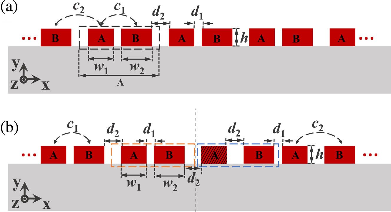
    Fig. 1. (a) Dimer chain with intra-dimer coupling strength c1 and inter-dimer coupling strength c2. Each dimer is composed of two waveguides, denoted as waveguides A and B. (b) Two dimer chains with distinct topological invariants are placed next to each other. The shadow waveguide A is with the waveguide number zero where the light inputs.
    Berry phase spectra for (a) c1/c2=5.51 and (b) c1/c2=0.182, with increasing η/c1.
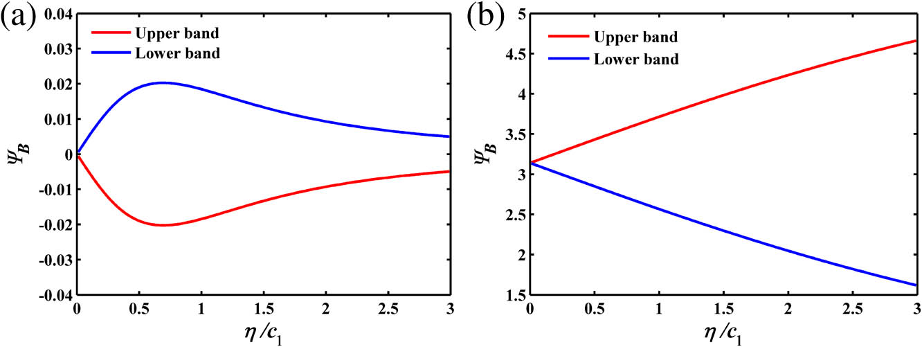
    Fig. 2. Berry phase spectra for (a) c1/c2=5.51 and (b) c1/c2=0.182, with increasing η/c1.
    (a) Eigen spectrum of the two-dimer-chain model illustrated in Fig. 1(b). The red “A” dot represents the topologically protected defect mode, and other dots (including the blue “B” dot and green “C” dot) represent the extended states. (b) Modal amplitude distribution of the topological defect mode, labeled the “A” dot in (a). (c), (d) Modal amplitude distribution of extended states, labeled the “B” dot and “C” dot in (a), respectively.
    Fig. 3. (a) Eigen spectrum of the two-dimer-chain model illustrated in Fig. 1(b). The red “A” dot represents the topologically protected defect mode, and other dots (including the blue “B” dot and green “C” dot) represent the extended states. (b) Modal amplitude distribution of the topological defect mode, labeled the “A” dot in (a). (c), (d) Modal amplitude distribution of extended states, labeled the “B” dot and “C” dot in (a), respectively.
    SEM images of the fabricated SOI waveguide arrays. (a) Two-dimer-chain structure. (b) Uniform array. The input waveguide merges into the center waveguide of the arrays.
    Fig. 4. SEM images of the fabricated SOI waveguide arrays. (a) Two-dimer-chain structure. (b) Uniform array. The input waveguide merges into the center waveguide of the arrays.
    (a), (c) Numerically simulated intensity distributions for light propagation in samples SWG-1 and SWG-2, respectively. (b), (d) Experimentally measured and simulated transmission at the output of samples SWG-1 and SWG-2, respectively.
    Fig. 5. (a), (c) Numerically simulated intensity distributions for light propagation in samples SWG-1 and SWG-2, respectively. (b), (d) Experimentally measured and simulated transmission at the output of samples SWG-1 and SWG-2, respectively.
    (a) Propagation constants of points A, E, and F as functions of the coupling ratio c1/c2. c2 is a variable, and other parameters are constants. (b) Modal amplitude distribution of the topological defect mode when c1/c2=1.2.
    Fig. 6. (a) Propagation constants of points A, E, and F as functions of the coupling ratio c1/c2. c2 is a variable, and other parameters are constants. (b) Modal amplitude distribution of the topological defect mode when c1/c2=1.2.
    Light field evolution for the disordered two-dimer-chain model.
    Fig. 7. Light field evolution for the disordered two-dimer-chain model.
    Tianying Lin, Ze Chen, Xiaopei Zhang, He Li, Xiaoping Liu, Haibin Lü. Experimental observation of topologically protected defect states in silicon waveguide arrays[J]. Chinese Optics Letters, 2020, 18(5): 051301
    Download Citation