Tianying Lin, Ze Chen, Xiaopei Zhang, He Li, Xiaoping Liu, Haibin Lü. Experimental observation of topologically protected defect states in silicon waveguide arrays[J]. Chinese Optics Letters, 2020, 18(5): 051301
Copy Citation Text
Photonic waveguide arrays provide a simple and versatile platform for simulating conventional topological systems. Here, we investigate a novel one-dimensional (1D) topological band structure, a dimer chain, consisting of silicon waveguides with alternating self-coupling and inter-coupling. Coupled mode theory is used to study topological features of such a model. It is found that topological invariants of our proposed model are described by the global Berry phase instead of the Berry phase of the upper or lower energy band, which is commonly used in the 1D topological models such as the Su–Schrieffer–Heeger model. Next, we design an array configuration composed of two dimer patterns with different global Berry phases to realize the topologically protected waveguiding. The topologically protected propagation feature is simulated based on the finite-difference time-domain method and then observed in the experiment. Our results provide an in-depth understanding of the dynamics of the topological defect state in a 1D silicon waveguide array, and may provide different routes for on-chip lightwave shaping and routing.
Photonic systems represent a promising platform for demonstrating novel quantum concepts and implementing quantum simulations[1–9] due to the mathematical isomorphism between the paraxial wave equation and the quantum Schrodinger equation[10]. Since the idea of topologically protected electromagnetic propagation was first, to the best of our knowledge, proposed[11,12] and subsequently experimentally verified in gyromagnetic media in the microwave regime[13], many topological concepts have been successfully extended to the optical regime (e.g., adiabatic pumping of light[14] and photonic topological insulators[15–18]). Notably, one-dimensional (1D) topological models [e.g., the Aubry–André–Harper (AAH) model[19] and the Su–Schrieffer–Heeger (SSH) model[20–23]] have attracted much attention due to relatively easy experiments and potentially promising applications in robust optical circuits. Among these 1D models, the SSH model unveiled in polyacetylene[20] presents the simplest topological band structure to describe the topologically protected states. The SSH model only consists of a chain of sites with alternating coupling (i.e., a dimer chain). It was revealed in Ref. [24] that the topologically protected states would appear in the interface between two different dimerization patterns with distinct topological invariants[25]. Such SSH photonic protected states have been demonstrated in coupled microwave cylindrical resonators[22], plasmonic waveguide arrays[21], and more recently ring-resonator arrays[26–28]. Lately, non-Hermitian modulations have also been introduced into the SSH model, leading to unique light propagation properties in these schemes[29–33].
In this Letter, we investigate the topological properties of a chain of waveguides with alternating self-coupling and inter-coupling. This scheme is different from the traditional cases with constant self-coupling (in other words, identical waveguides)[21–23]. It is found that the topological invariants of our system are described by the Berry phase of neither the upper nor lower energy band but their sum. Coupled mode theory (CMT) is applied to investigate the dynamics of the topological defect bound state, emerging at the interface between two dimer chains with distinct global Berry phases, which is experimentally observed in a silicon-on-insulator (SOI) photonic integrated platform.
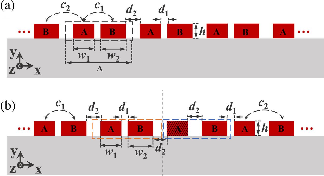
A superstructure unit formed by two different waveguides is used to construct a dimer chain, as shown in Fig. 1(a). For the sake of simplicity, the individual waveguide in our system considered here is assumed to support only a fundamental mode. Since the waveguides are different in width, their fundamental modes are different in propagation constants or self-coupling. Under the tight-binding approximation[34], the coupled mode equations with nearest neighbor coupling can be expressed as where is the propagation distance, and are the modal amplitudes of waveguides A and B at the th dimer, respectively, and represent the corresponding propagation constants, respectively, and and are the intra-dimer and inter-dimer coupling strengths, respectively. The corresponding Bloch Hamiltonian[30,31,35] is where , is the period, and is the quasi-momentum in the Brillouin zone. By defining in a new form , the eigenvalues and associated eigenvectors of Eq. (3) are obtained: where , and . Berry phases of the upper and lower energy bands are given by[24,36]
Sign up for Chinese Optics Letters TOC. Get the latest issue of Chinese Optics Letters delivered right to you!Sign up now
Figure 1.(a) Dimer chain with intra-dimer coupling strength and inter-dimer coupling strength . Each dimer is composed of two waveguides, denoted as waveguides A and B. (b) Two dimer chains with distinct topological invariants are placed next to each other. The shadow waveguide A is with the waveguide number zero where the light inputs.
If , this model is exactly the well-known SSH model[20–23], and it can be obtained that based on Eq. (7). The topological nature of this system is identified by (or ), which is zero if and if . In contrast, when , (or ) varies continuously with increasing , so it cannot be regarded as the topological invariant. The typical curves of under the conditions of (for example, ) and (for example, ) are shown in Figs. 2(a) and 2(b), respectively. It, however, can be found from Eq. (7) that the second terms of can cancel each other. Therefore, we can define a new physical quantity, the global Berry phase, as follows:
Figure 2.Berry phase spectra for (a) and (b) , with increasing .
The value of does not depend on the values of (except the abrupt change at the topological transition point ) and , implying that the topological invariant for this system can be described by this global Berry phase.
A silicon photonic waveguide array on an SOI platform is designed to study the topologically protected wave propagation based on the aforementioned dimer chain model. This array structure [see Fig. 1(b)] consists of two neighboring dimer chains with distinct global Berry phases. The large contrast between the inter-dimer and intra-dimer coupling is required to guarantee the strong topological protection effect and the tight defect mode field confinement in the center waveguide[21–23]. However, the minimum separation between waveguides is restricted by the minimum feature size defined by the fabrication process, so as to avoid proximity effects. The other separation parameter can be determined by the characteristics of the induced desired defect mode (which would be discussed in detail at the end of the article). With these considerations, the parameters of this system are chosen as follows: width of waveguide A , width of waveguide B , height and length of both waveguides and , and the total number of waveguides . The refractive index of the silicon waveguides (SWGs), silica substrate, and air cladding at 1500 nm used in our simulations is 3.48, 1.44, and 1, respectively. The distance between waveguides, as shown in Fig. 1, is chosen as and , respectively. The corresponding propagation constants and coupling strengths simulated by the finite-difference time-domain (FDTD) method are , , , and . The field propagation within the waveguide array can be described using the CMT method as[37–40]where , and represents the modal amplitude in the th waveguide. The calculated eigenvalue diagrams are shown in Fig. 3(a). There are two bands separated by a bandgap, where there exists a topological defect state (the red “A” dot). The emergence of the defect state is due to the topological transition at the interface[21–23]. The midgap defect state shown in Fig. 3(a) is protected by its isolation from bulk states, and the isolation corresponds to the topological arrangement of the structure, implying that the defect mode is topologically protected. To highlight the property of this defect state, the modal amplitudes of this state and two arbitrarily chosen extended states (blue “B” dot and green “C” dot) are depicted in Figs. 3(b)–3(d), respectively. Clearly, the electric field of the defect state is tightly confined on the central waveguide, while the fields of the extended states appear to be distributed in almost all of the waveguides.
Figure 3.(a) Eigen spectrum of the two-dimer-chain model illustrated in Fig. 1(b). The red “A” dot represents the topologically protected defect mode, and other dots (including the blue “B” dot and green “C” dot) represent the extended states. (b) Modal amplitude distribution of the topological defect mode, labeled the “A” dot in (a). (c), (d) Modal amplitude distribution of extended states, labeled the “B” dot and “C” dot in (a), respectively.
The two-dimer-chain topological structure is fabricated on an SOI wafer with a 220 nm thick top silicon layer and a 2 μm buried silicon-dioxide buffer layer using electronic beam lithography and inductively coupled plasma reactive ion etching. The scanning electron micrograph (SEM) images of this topologically non-trivial sample [defined as SWG array (SWA-1)] are shown in Fig. 4(a). In order to highlight the light behavior in sample SWA-1, we have also fabricated another topologically trivial sample (defined as SWA-2), shown in Fig. 4(b), for comparison, by changing the waveguide spacing to a uniform one (), while keeping other parameters the same as those of sample SWA-1. Light in-coupling is realized via a grating coupler on the central input waveguide, while light out-coupling is realized on the nine central output waveguides also via grating couplers.
Figure 4.SEM images of the fabricated SOI waveguide arrays. (a) Two-dimer-chain structure. (b) Uniform array. The input waveguide merges into the center waveguide of the arrays.
The light propagations in samples SWA-1 and SWA-2 are numerically simulated based on the FDTD method, and the obtained results are shown in Figs. 5(a) and 5(c), respectively. In particular, the topological defect bound state is successfully observed, which remains localized in the central waveguide during propagation. This kind of behavior is consistent with the modal field distribution analyzed by CMT, as shown with the bar graph in Fig. 3(b). Notice that there is slight field spreading to the next nearest neighbor waveguides on both sides due to propagation phase matching [see Figs. 3(a) and 3(b)]. In contrast, in the topologically trivial equidistance waveguide array, light spreads out as it propagates, and much of the light is concentrated in two outer side lobes, as shown in Fig. 5(c). Notice that the light is reflected at the boundary of this waveguide array with the propagation distance of ∼700 μm. This diffusive behavior of light is well described by the “discrete diffraction” revealed in Refs. [41,42].
Figure 5.(a), (c) Numerically simulated intensity distributions for light propagation in samples SWG-1 and SWG-2, respectively. (b), (d) Experimentally measured and simulated transmission at the output of samples SWG-1 and SWG-2, respectively.
The experimentally measured transmission of the central nine waveguides of SWG-1 is depicted using the blue bars in Fig. 5(b). It is confirmed experimentally that most of the light remains in the central waveguide (), proving the existence of the topological defect state. In contrast, the measured transmission profile of SWG-2 indicates that there is very little power at the output of the nine central waveguides (almost 40 times smaller compared with that in SWG-1). The overall light propagation trend is consistent with the results predicted by FDTD simulations in Figs. 5(b) and 5(d) (see the red bars). The slight deviation between the experimental results and the simulation ones is mostly attributed to the fabrication imperfection. Nevertheless, these results suggest that the propagation behavior of light can be drastically changed by engineering unique topological features in the waveguide arrays.
Here, we would like to investigate the relation between the propagation constants of points A, E, and F illustrated in Fig. 3(a) and the inter-waveguide coupling ratio (). As shown in Fig. 6(a), the gap between points A and E, and the gap between points A and F increase as increases. The big gap reflects the big propagation constant difference between the defect mode and the bulk modes. Thus, the choice of the large coupling ratio () in this manuscript is to ensure the strong topological protection effect of the defect mode, since it is difficult for the defect mode to be coupled with other modes under perturbation, such as the inevitable fabrication error. Moreover, as shown in Fig. 3(b), the electric field of the defect state is tightly confined on the central waveguide, and thus the defect mode is easily excited and observed in the experiment. In contrast, the small coupling ratio is undesired, since the defect mode is less robust to perturbation and more difficult to be excited and observed experimentally due to more diffused modal field distribution, as shown in Fig. 6(b). It is also found that the propagation constant of the defect state is not affected by the inter-waveguide coupling ratio () and is exactly equal to the propagation constant of the fundamental mode of the center waveguide, which may be due to the nature of the topological transition interface. Such a defect mode is also called the topological zero mode in Refs. [21,32].
Figure 6.(a) Propagation constants of points A, E, and F as functions of the coupling ratio . is a variable, and other parameters are constants. (b) Modal amplitude distribution of the topological defect mode when .
Finally, the topological protection effect of this structure is verified by testing its robustness against the structural disorder. The structural disorder is introduced by defining the waveguide separations as[21,32]where is the disorder strength corresponding to the maximum fabrication error. Here, is chosen as 15 nm, and is a random number uniformly distributed in the interval , influencing the th unit cell. The random variables in the th and the th unit cells, and , are independent if . As shown in Fig. 7, the non-spreading property of light propagation is almost maintained, implying the robustness of the structure to the disorder.
Figure 7.Light field evolution for the disordered two-dimer-chain model.
In summary, we investigate a 1D topological band structure, the superstructure dimer chain, of which the unit cell consists of two different SWGs with different widths. In this unique system, the topological invariant is described by the global Berry phase rather than the Berry phase of the individual energy band that is commonly used in the 1D topological models such as the SSH model. An on-chip silicon photonic waveguide array with different global Berry phases is designed to implement our theoretical model. Topologically protected propagation is observed experimentally as a localized interface state. Our results could help deepen the understanding of topological properties of 1D coupled waveguide arrays, and may have potential applications in on-chip information routing and processing. Besides, our results pave the way towards novel approaches to localize light on the interface between two photonic crystals and may apply to adiabatic pumping of light[14], and the concept of the corresponding interface states can be extended to higher-dimensional systems with alternating self-coupling and inter-coupling.
Tianying Lin, Ze Chen, Xiaopei Zhang, He Li, Xiaoping Liu, Haibin Lü. Experimental observation of topologically protected defect states in silicon waveguide arrays[J]. Chinese Optics Letters, 2020, 18(5): 051301