• Journal of Semiconductors
  • Vol. 43, Issue 9, 092501 (2022)
Jingzhi Fang1、2、3、4, Huading Song3, Bo Li5, Ziqi Zhou1、2、3, Juehan Yang1、2, Benchuan Lin4, Zhimin Liao3、*, and Zhongming Wei1、2、**
Author Affiliations
  • 1State Key Laboratory of Superlattices and Microstructures, Institute of Semiconductors, Chinese Academy of Sciences, Beijing 100083, China
  • 2Center of Materials Science and Optoelectronics Engineering, University of Chinese Academy of Sciences, Beijing 100049, China
  • 3State Key Laboratory for Mesoscopic Physics and Frontiers Science Center for Nano-optoelectronics, School of Physics, Peking University, Beijing 100871, China
  • 4Shenzhen Institute for Quantum Science and Engineering, Southern University of Science and Technology, Shenzhen 518055, China
  • 5Hunan Key Laboratory of Two-Dimensional Materials, Department of Applied Physics, School of Physics and Electronics, Hunan University, Changsha 410082, China
  • show less
    DOI: 10.1088/1674-4926/43/9/092501 Cite this Article
    Jingzhi Fang, Huading Song, Bo Li, Ziqi Zhou, Juehan Yang, Benchuan Lin, Zhimin Liao, Zhongming Wei. Large unsaturated magnetoresistance of 2D magnetic semiconductor Fe-SnS2 homojunction[J]. Journal of Semiconductors, 2022, 43(9): 092501 Copy Citation Text show less
    (Color online) Characterization of the Fe-SnS2 flakes. (a) The atomic structure of Fe-SnS2. One Sn atom is replaced by one Fe atom and surrounded by six Sn atoms. (b) Raman spectra of Fe-SnS2 and SnS2 flakes. (c) EDS of the Fe-SnS2 flake. Inset is a partially enlarged view of the characteristic peaks of Fe. (d) Low-resolution TEM image of the Fe-SnS2 flake. (e) High resolution TEM image of Fe-SnS2 flake. (f) SAED patterns of Fe-SnS2 flake.
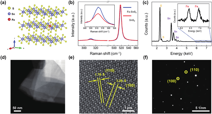
    Fig. 1. (Color online) Characterization of the Fe-SnS2 flakes. (a) The atomic structure of Fe-SnS2. One Sn atom is replaced by one Fe atom and surrounded by six Sn atoms. (b) Raman spectra of Fe-SnS2 and SnS2 flakes. (c) EDS of the Fe-SnS2 flake. Inset is a partially enlarged view of the characteristic peaks of Fe. (d) Low-resolution TEM image of the Fe-SnS2 flake. (e) High resolution TEM image of Fe-SnS2 flake. (f) SAED patterns of Fe-SnS2 flake.
    (Color online) (a) Schematic diagram of Fe-SnS2 homojunction device. (b) AFM image of a typical device. On the right-hand is the corresponding optical microscope image, and the relative direction of the applied magnetic field is marked. The scale is 5μm. (c)I–Vds curves at zero magnetic field, 14 T vertical magnetic field and 14 T parallel magnetic field. The inset is an enlarged view of the conduction part.
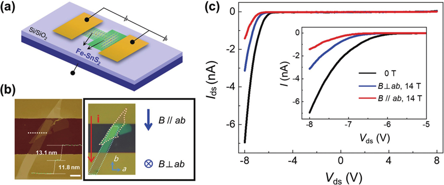
    Fig. 2. (Color online) (a) Schematic diagram of Fe-SnS2 homojunction device. (b) AFM image of a typical device. On the right-hand is the corresponding optical microscope image, and the relative direction of the applied magnetic field is marked. The scale is 5μm. (c)IVds curves at zero magnetic field, 14 T vertical magnetic field and 14 T parallel magnetic field. The inset is an enlarged view of the conduction part.
    (Color online) MR of the Fe-SnS2 homojunction device under parallel magnetic field. (a)I–Vds curves under different magnetic fields. (b) Dependence of MR on magnetic field extracted fromIds–B curves atVds = –7 V. (c) Extracted MR as a function of bias based on theI–Vds curves at zero magnetic field and 14 T. There is a peak value of MR atVds ~ –6.5 V.
    Fig. 3. (Color online) MR of the Fe-SnS2 homojunction device under parallel magnetic field. (a)IVds curves under different magnetic fields. (b) Dependence of MR on magnetic field extracted fromIdsB curves atVds = –7 V. (c) Extracted MR as a function of bias based on theIVds curves at zero magnetic field and 14 T. There is a peak value of MR atVds ~ –6.5 V.
    (Color online) MR of the Fe-SnS2 homojunction device under vertical magnetic field. (a)I–Vds curves under different magnetic fields. (b) Dependence of MR on magnetic field extracted fromIds–B curves atVds = –7 V. The magnetic field direction is vertical to the device plane. (c) Extracted MR as a function of bias based on theI–Vds curves at zero magnetic field and 14 T. There is a peak value of MR atVds ~ –6.2 V.
    Fig. 4. (Color online) MR of the Fe-SnS2 homojunction device under vertical magnetic field. (a)IVds curves under different magnetic fields. (b) Dependence of MR on magnetic field extracted fromIdsB curves atVds = –7 V. The magnetic field direction is vertical to the device plane. (c) Extracted MR as a function of bias based on theIVds curves at zero magnetic field and 14 T. There is a peak value of MR atVds ~ –6.2 V.
    (Color online)Vg dependence of the Fe-SnS2 homojunction device.I–Vds curves under different gate voltages in (a) parallel and (b) vertical magnetic fields. The black line is the curve at 14 T and the red line is the curve at zero magnetic field. At large negativeVg (–8 V and –5 V), MR tends to infinity under parallel magnetic field.
    Fig. 5. (Color online)Vg dependence of the Fe-SnS2 homojunction device.IVds curves under different gate voltages in (a) parallel and (b) vertical magnetic fields. The black line is the curve at 14 T and the red line is the curve at zero magnetic field. At large negativeVg (–8 V and –5 V), MR tends to infinity under parallel magnetic field.
    Jingzhi Fang, Huading Song, Bo Li, Ziqi Zhou, Juehan Yang, Benchuan Lin, Zhimin Liao, Zhongming Wei. Large unsaturated magnetoresistance of 2D magnetic semiconductor Fe-SnS2 homojunction[J]. Journal of Semiconductors, 2022, 43(9): 092501
    Download Citation