Author Affiliations
1State Key Laboratory of Superlattices and Microstructures, Institute of Semiconductors, Chinese Academy of Sciences, Beijing 100083, China2Center of Materials Science and Optoelectronics Engineering, University of Chinese Academy of Sciences, Beijing 100049, China3State Key Laboratory for Mesoscopic Physics and Frontiers Science Center for Nano-optoelectronics, School of Physics, Peking University, Beijing 100871, China4Shenzhen Institute for Quantum Science and Engineering, Southern University of Science and Technology, Shenzhen 518055, China5Hunan Key Laboratory of Two-Dimensional Materials, Department of Applied Physics, School of Physics and Electronics, Hunan University, Changsha 410082, Chinashow less
Abstract
A magnetic semiconductor whose electronic charge and spin can be regulated together will be an important component of future spintronic devices. Here, we construct a two-dimensional (2D) Fe doped SnS2 (Fe-SnS2) homogeneous junction and investigate its electromagnetic transport feature. The Fe-SnS2 homojunction device showed large positive and unsaturated magnetoresistance (MR) of 1800% in the parallel magnetic field and 600% in the vertical magnetic field, indicating an obvious anisotropic MR feature. In contrast, The MR of Fe-SnS2 homojunction is much larger than the pure diamagnetic SnS2 and most 2D materials. The application of a gate voltage can regulate the MR effect of Fe-SnS2 homojunction devices. Moreover, the stability of Fe-SnS2 in air has great application potential. Our Fe-SnS2 homojunction has a significant potential in future magnetic memory applications.A magnetic semiconductor whose electronic charge and spin can be regulated together will be an important component of future spintronic devices. Here, we construct a two-dimensional (2D) Fe doped SnS2 (Fe-SnS2) homogeneous junction and investigate its electromagnetic transport feature. The Fe-SnS2 homojunction device showed large positive and unsaturated magnetoresistance (MR) of 1800% in the parallel magnetic field and 600% in the vertical magnetic field, indicating an obvious anisotropic MR feature. In contrast, The MR of Fe-SnS2 homojunction is much larger than the pure diamagnetic SnS2 and most 2D materials. The application of a gate voltage can regulate the MR effect of Fe-SnS2 homojunction devices. Moreover, the stability of Fe-SnS2 in air has great application potential. Our Fe-SnS2 homojunction has a significant potential in future magnetic memory applications.Introduction
The magnetoresistance (MR) effect has always been a very important research direction in the field of condensed matter. Taking the giant MR (GMR) effect as an example, the research of MR is of great significance in the field of magnetic storage and so on. For a long time, from ordinary MR (OMR) and GMR, to colossal MR (CMR) and even larger, researchers have been committed to finding materials with larger MR and better performance to meet the needs of practical device applications. Tunneling MR (TMR) has also made a lot of progress with the development of magnetic multilayers and 2D materials[1-4]. Among the traditional materials, researchers have tended to use metal materials to prepare magnetic devices with more prominent properties through the regulation of the magnetic layer and insulating layer[5,6]. Furthermore, very large unsaturated MR has been found in some systems, and the positive MR was up to 103%–108%. These systems are mainly metal and semi-metallic materials, some of which have topological properties and have great research prospects[7,8].
Over the last decade, with the successful synthesis and exfoliation of a variety of 2D materials, the study of 2D magnetic materials has attracted wide attention. The doping of impurity atoms is one of the most commonly means of semiconductor function regulation. This is similar to the growth of diluted magnetic semiconductor (DMS)[9-11]. In the past few years, researchers have realized the doping of a variety of transition metal dichalcogenides (TMDs) materials by material growth methods such as chemical vapor deposition (CVD)[12,13]. The adjustment of band-gap and carrier concentration by impurity doping has achieved very important applications in the field of optoelectronics[14]. Similarly, the introduction of magnetism into non-ferromagnetic 2D TMDs through the doping of magnetic atoms is one of the researched orientations[15-18]. For example, MoS2 has been doped with transition metal atoms, such as Fe and Co[19,20]. However, research on magnetic doped TMDs has focused more on material growth and increasing Curie temperature[21-26].
With the further study of magnetic materials, 2D intrinsic magnetic materials have been successfully synthesized, such as antiferromagnetic materials CrI3[27-30], FePS3[31], ferromagnetic materials Cr2Ge2Te6[32-35], Fe3GeTe2[36,37], VSe2[38], etc. A large number of original studies have been carried out from the magnetic research related to the number of layers[30], the regulation of magnetic order[34], and then to spintronic devices[39]. It is worth noting that the magnetic tunnel junction (MTJ) prepared with thin layer CrI3 as spin filtering tunnel barrier can obtain considerable tunneling magnetoresistance (TMR)[40]. At low temperature (2 K) in a four-layer CrI3 spin-filter magnetic tunnel junction (sf-MTJ), the TMR reaches an amazing 190000%. In addition, the anisotropy of MR is one of the characteristics of ferromagnets. In CrI3 sf-MTJ, the sf-TMR for in-plane magnetization is larger than that for out-of-plane, which is related to the anisotropic spin-orbit coupling produced by CrI3 layered structure. Meanwhile, asymmetry in positive and negative bias is found in the literature, which are attributed to different thickness and coercivity fields similar to those of EuS sf-MTJ[2].
However, it is regrettable that most 2D materials with intrinsic magnetism are unstable and extremely sensitive to air, which is a problem that cannot be ignored. Although commendable progress has been made in the research of intrinsic magnetic materials and devices, it is still a very promising direction to realize more functions in doped magnetic 2D semiconductors. Taking Fe doped SnS2 material as an example, long-range ferromagnetic ordering is realized while maintaining high optoelectronic performance, while it still maintains excellent air stability[17]. These characteristics show that magnetic doped 2D magnetic semiconductor materials have a unique application potential in spintronics.
In this work, we investigate the homojunction established by Fe atom doped 2D semiconductor material SnS2 (hereinafter referred to as Fe-SnS2)[17,41]. The homojunction device obtained a high MR ~ 1800% in parallel magnetic field (B//) and MR ~ 600% in vertical magnetic field (B⊥), which shows the large anisotropic MR effect.
Experiment and method
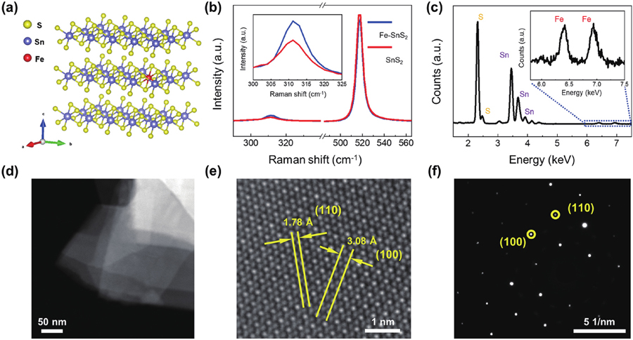
A Fe-SnS2 single crystal was grown by chemical vapor transport (CVT) method, and the atomic proportion of Fe is ~ 2.1% (i.e., Fe0.021Sn0.979S2). Few-layer Fe-SnS2 were obtained by mechanical exfoliation. Fe atoms are substituted doped at Sn position [Fig. 1(a)][17]. Raman spectroscopy has been widely used in 2D materials to characterize their crystallinity, composition and doping. The Raman spectrum of Fe-SnS2 shows one peak at 311 cm–1, which corresponds to theA1g mode and is broader than the pure SnS2 [Fig. 1(b)]. This behavior is consistent with that in the monolayer[9] and other 2D alloys[42]. The characteristic peaks of Sn, S, and Fe are identified in the energy-dispersive X-ray spectroscopy (EDS) of the Fe-SnS2 flake, which confirms the existence of Fe doping [Fig. 1(c)].Fig. 1(d) shows a low-resolution high resolution transmission electron microscopy (TEM) image of a few-layer Fe-SnS2. TEM [Fig. 1(e)] and the corresponding selected area electron diffraction (SAED) [Fig. 1(f)] reveal that the Fe-SnS2 nanosheet has lattice spacing of 0.308 and 0.178 nm assigned to the (100) and (110) planes along the [001] zone axis, showing a high-quality hexagonal symmetry structure [Fig. 1(d) and1(e)].

Figure 1.(Color online) Characterization of the Fe-SnS2 flakes. (a) The atomic structure of Fe-SnS2. One Sn atom is replaced by one Fe atom and surrounded by six Sn atoms. (b) Raman spectra of Fe-SnS2 and SnS2 flakes. (c) EDS of the Fe-SnS2 flake. Inset is a partially enlarged view of the characteristic peaks of Fe. (d) Low-resolution TEM image of the Fe-SnS2 flake. (e) High resolution TEM image of Fe-SnS2 flake. (f) SAED patterns of Fe-SnS2 flake.
Few-layer Fe-SnS2 flakes were exfoliated by scotch tape or polydimethylsiloxane (PDMS). Then, the homojunction devices were established by PDMS-assisted dry transfer method, and the metal electrodes were prepared by electron beam evaporation or thermal evaporation [Fig. 2(a)]. The contact of the devices was improved by annealing. In this work, the thickness of flakes of typical devices is 10–40 nm, which was characterized by atomic force microscopy (AFM).Fig. 2(b) shows the AFM image of a typical device (left-hand) and the corresponding optical microscope (OM) image (the right), in which the relative direction of the applied magnetic field is marked.
Figure 2.(Color online) (a) Schematic diagram of Fe-SnS2 homojunction device. (b) AFM image of a typical device. On the right-hand is the corresponding optical microscope image, and the relative direction of the applied magnetic field is marked. The scale is 5μm. (c)I–Vds curves at zero magnetic field, 14 T vertical magnetic field and 14 T parallel magnetic field. The inset is an enlarged view of the conduction part.
Results and discussion
The transport properties of the devices were measured by an Oxford refrigerator. Our previous report demonstrated that the Curie temperature of Fe0.021Sn0.979S2 is ~31 K[17]. Because the influence of thermal disturbance on electromagnetic transport can be greatly reduced at low temperature, all of our data were measured at 1.6 K. The relationship between source–drain current (Ids) and DC bias voltage (Vds) of the Fe-SnS2 homojunction device was measured under magnetic field of zero and 14 T in the direction vertical toab plane (B⊥ab) and parallel toab plane (B//ab) [Fig. 2(c)]. First, the electromagnetic transport of the Fe-SnS2 homojunction device inB//ab was investigated carefully. TheIds–Vds curves under different magnetic fields in a parallel magnetic field indicate that the magnetic field suppresses the current monotonically [Fig. 3(a)]. The MR can be obtained using the formula:
Figure 3.(Color online) MR of the Fe-SnS2 homojunction device under parallel magnetic field. (a)I–Vds curves under different magnetic fields. (b) Dependence of MR on magnetic field extracted fromIds–B curves atVds = –7 V. (c) Extracted MR as a function of bias based on theI–Vds curves at zero magnetic field and 14 T. There is a peak value of MR atVds ~ –6.5 V.
where
and
are the resistivity under applied magnetic field and zero magnetic field, respectively. One typical MR curve underVds of –7 V shows that MR still did not reach saturation when the magnetic field reached a maximum of 14 T [Fig. 3(b)]. Comparing theI–Vds curve at 14 T with that at zero magnetic field, it is found that the MR can reach ~1800% atVds ~ –6.5 V [Fig. 3(c)], which is larger than that of SnS2 homojunction of 40% (Fig. S3). The large MR of the Fe-SnS2 homojunction should result from the scattering of electrons induced by the Lorentz force in the magnetic field and partial magnetic state transition of the homojunction. The Lorentz force is positively correlated with the magnetic field and can induce the electron collision probability, thus increase the MR. Meanwhile, due to the low doping rate of Fe atoms and weak magnetism, the magnetic state transition should be partial, which leads to unsaturated MR. As theVds increases, the MR first increases and then decreases [Fig. 3(c)], which will be explained as follows: at lowVds, the electrons are not driven and move enough, and the electron scattering is small, thus the MR is small. With the increase ofVds, the electrons move and the scattering increases gradually. When theVds continues to increase, the MR of electrons will be reduced because the electric field force is enhanced and the scattering induced by Lorentz force is relatively small.
The electromagnetic transport of the Fe-SnS2 homojunction device inB⊥ab was then investigated.Fig. 4(a) shows a magnetic field suppression conductive behavior similar to that under a parallel magnetic field. The MR increased with the increasing magnetic field and showed unsaturated behavior [Fig. 4(b)]. Comparing theI–Vds curve at 14 T with that at zero magnetic field, the maximum MR of ~ 600% can be obtained atVds of –6.2 V [Fig. 4(c)], which is larger than that of SnS2 homojunction of 80% (Fig. S4). AlongB//ab andB⊥ab directions, the maximum MR ratio is 3, indicating the obvious anisotropic MR of Fe-SnS2 homojunction. The anisotropic MR here should come from the magnetic anisotropy of Fe-SnS2, which can produce anisotropic electron magnetic scattering. In addition, in our work, the asymmetry behavior of positive and negative bias voltage is similar to that in CrI3 sf-MTJ[2]. Aside from the difference between the two Fe-SnS2 flakes of the thickness and coercive field, we consider that there is additional charge accumulation caused by magnetic interaction at the interface between the two flakes. Therefore, there are large differences between positive and negative bias voltages, and even a unidirectional conductive behavior is produced.
Figure 4.(Color online) MR of the Fe-SnS2 homojunction device under vertical magnetic field. (a)I–Vds curves under different magnetic fields. (b) Dependence of MR on magnetic field extracted fromIds–B curves atVds = –7 V. The magnetic field direction is vertical to the device plane. (c) Extracted MR as a function of bias based on theI–Vds curves at zero magnetic field and 14 T. There is a peak value of MR atVds ~ –6.2 V.
We then added gate voltage (Vg) regulation (Fig. 5). It is worth noting that when a large negative gate voltage (–8 V) was applied, the unidirectional conduction direction of the current could be changed. Furthermore, the application ofVg could regulate the MR. As shown inFig. 5,Figs. 5(a) and5(b) areI–Vds curves related toVg and magnetic field under parallel and vertical magnetic fields, respectively. Interestingly, under the parallel magnetic field, when a largeVg [Vg = –8 V and –5 V in theFig. 5(a)] is applied, the magnetic field could adjust the device to the off-state (shown here as almost non-conductive). The results of vertical magnetic field are almost consistent with those of parallel magnetic field, but the MR is always smaller. Meanwhile, when the positiveVg increases continuously (Fig. S2) and the MR was suppressed, as shown inFig. 5 (Vg = 5 V and 8 V). This phenomenon should be related to the regulation of carrier concentration by gate voltage, which changes the scattering probability. We have given this further consideration in the supplementary materials.
Figure 5.(Color online)Vg dependence of the Fe-SnS2 homojunction device.I–Vds curves under different gate voltages in (a) parallel and (b) vertical magnetic fields. The black line is the curve at 14 T and the red line is the curve at zero magnetic field. At large negativeVg (–8 V and –5 V), MR tends to infinity under parallel magnetic field.
Conclusion
In conclusion, we first characterized the Fe atom doped SnS2 material. The results of Raman, and TEM show that Fe-SnS2 has high crystal quality. We then established the homojunction device using Fe-SnS2 flakes and measured the low-temperature transport. We obtained MR ~1800% in parallel magnetic field (B‖) and MR ~600% in vertical magnetic field (B⊥), indicating obvious anisotropic MR feature. This is in obvious contrast to the MR of pure diamagnetic SnS2 material. The application of gate voltage could regulate the MR effect of Fe-SnS2 homojunction devices. Finally, our Fe-SnS2 homojunction has significant potential in future magnetic memory applications.
Acknowledgements
This work was financially supported by the National Key Research and Development Program of China (Grant No. 2017YFA0207500), the National Natural Science Foundation of China (Grant No. 62125404), the Strategic Priority Research Program of Chinese Academy of Sciences (Grant No. XDB43000000).
Appendix A. Supplementary materials
Supplementary materials to this article can be found online athttps://doi.org/10.1088/1674-4926/43/9/092501.
References
[1] C Gong, X Zhang. Two-dimensional magnetic crystals and emergent heterostructure devices. Science, 363, 706(2019).
[2] T Song, X Cai, M W Tu et al. Giant tunneling magnetoresistance in spin-filter van der Waals heterostructures. Science, 360, 1214(2018).
[3] S Bhatti, R Sbiaa, A Hirohata et al. Spintronics based random access memory: a review. Mater Today, 20, 530(2017).
[4] Z Wang, I Gutierrez-Lezama, N Ubrig et al. Very large tunneling magnetoresistance in layered magnetic semiconductor CrI3. Nat Commun, 9, 2516(2018).
[5] S Ikeda, J Hayakawa, Y Ashizawa et al. Tunnel magnetoresistance of 604% at 300 K by suppression of Ta diffusion in CoFeB/MgO/CoFeB pseudo-spin-valves annealed at high temperature. Appl Phys Lett, 93, 082508(2008).
[6] S Ikeda, K Miura, H Yamamoto et al. A perpendicular-anisotropy CoFeB-MgO magnetic tunnel junction. Nat Mater, 9, 721(2010).
[7] R Niu, W Zhu. Materials and possible mechanisms of extremely large magnetoresistance: a review. J Phys: Condens Matter, 34, 113001(2022).
[8] M Ali, J Xiong, S Flynn et al. Large, non-saturating magnetoresistance in WTe2. Nature, 514, 205(2014).
[9] T Dietl, H Ohno. Dilute ferromagnetic semiconductors: Physics and spintronic structures. Rev Mod Phys, 86, 187(2014).
[10] T Dietl. A ten-year perspective on dilute magnetic semiconductors and oxides. Nat Mater, 9, 965(2010).
[11] A Ramasubramaniam, D Naveh. Mn-doped monolayer MoS2: An atomically thin dilute magnetic semiconductor. Phys Rev B, 87, 195201(2013).
[12] L Loh, Z Zhang, M Bosman et al. Substitutional doping in 2D transition metal dichalcogenides. Nano Res, 14, 1668(2021).
[13] A A Tedstone, D J Lewis, P O’Brien. Synthesis, properties, and applications of transition metal-doped layered transition metal dichalcogenides. Chem Mater, 28, 1965(2016).
[14] J Z Fang, Z Z Zhou, M Q Xiao et al. Recent advances in low-dimensional semiconductor nanomaterials and their applications in high-performance photodetectors. InfoMat, 2, 291(2019).
[15] M Hossain, B Qin, B Li et al. Synthesis, characterization, properties and applications of two-dimensional magnetic materials. Nano Today, 42, 101338(2022).
[16] V Kochat, A Apte, J A Hachtel et al. Re Doping in 2D transition metal dichalcogenides as a new route to tailor structural phases and induced magnetism. Adv Mater, 29, 1703754(2017).
[17] B Li, T Xing, M Z Zhong et al. A two-dimensional Fe-doped SnS2 magnetic semiconductor. Nat Commun, 8, 1958(2017).
[18] H Bouzid, R Sahoo, S J Yun et al. Multiple magnetic phases in van der Waals Mn-doped SnS2 semiconductor. Adv Func Mater, 31, 2102560(2021).
[19] B Li. Huang L, Zhong M Z, et al. Synthesis and transport properties of large-scale alloy Co0.16Mo0.84S2 bilayer nanosheets. ACS Nano, 9, 1257(2015).
[20] J Zhou, J Lin, H Sims et al. Synthesis of Co-doped MoS2 monolayers with enhanced valley splitting. Adv Mater, 32, 1906536(2020).
[21] P M Coelho, H Komsa, K Lasek et al. Room-temperature ferromagnetism in MoTe2 by post-growth incorporation of vanadium impurities. Adv Elec Mater, 5, 1900044(2019).
[22] S Fu, K Kang, K Shayan et al. Enabling room temperature ferromagnetism in monolayer MoS2 via in situ iron-doping. Nat Commun, 11, 2034(2020).
[23] Y T H Pham, M Liu, V O Jimenez et al. Tunable ferromagnetism and thermally induced spin flip in vanadium-doped tungsten diselenide monolayers at room temperature. Adv Mater, 32, 2003607(2020).
[24] L Yang, H Wu, W Zhang et al. Ta doping enhanced room-temperature ferromagnetism in 2D semiconducting MoTe2 nanosheets. Adv Electrin Mater, 5, 1900552(2019).
[25] S J Yun, D L Duong, D M Ha et al. Ferromagnetic order at room temperature in monolayer WSe2 semiconductor via vanadium dopant. Adv Sci, 7, 1903076(2020).
[26] F Zhang, B Zheng, A Sebastian et al. Monolayer vanadium-doped tungsten disulfide: A room-temperature dilute magnetic semiconductor. Adv Sci, 7, 2001174(2020).
[27] B Huang, G Clark, D Klein et al. Electrical control of 2D magnetism in bilayer CrI3. Nat Nanotech, 13, 544(2018).
[28] S Jiang, L Li, Z Wang et al. Controlling magnetism in 2D CrI3 by electrostatic doping. Nat Nanotech, 13, 549(2018).
[29] S Jiang, J Shan, K F Mak. Electric-field switching of two-dimensional van der Waals magnets. Nat Mater, 17, 406(2018).
[30] B Huang, G Clark, E Navarro-Moratalla et al. Layer-dependent ferromagnetism in a van der Waals crystal down to the monolayer limit. Nature, 546, 270(2017).
[31] J U Lee, S Lee, J H Ryoo et al. Ising-type magnetic ordering in atomically thin FePS3. Nano Lett, 16, 7433(2016).
[32] C Gong, L Li, Z Li et al. Discovery of intrinsic ferromagnetism in two-dimensional van der Waals crystals. Nature, 546, 265(2017).
[33] W Xing, Y Chen, P M Odenthal et al. Electric field effect in multilayer Cr2Ge2Te6: a ferromagnetic 2D material. 2D Mater, 4, 2053(2017).
[34] Z Wang, T Zhang, M Ding et al. Electric-field control of magnetism in a few-layered van der Waals ferromagnetic semiconductor. Nat Nanotech, 13, 554(2018).
[35] M Mogi, A Tsukazaki, Y Kaneko et al. Ferromagnetic insulator Cr2Ge2Te6 thin films with perpendicular remanence. APL Mater, 6, 091104(2018).
[36] Y J Deng, Y J Yu, Y C Song et al. Gate-tunable room-temperature ferromagnetism in two-dimensional Fe3GeTe2. Nature, 563, 94(2018).
[37] Z Fei, B Huang, P Malinowski et al. Two-dimensional itinerant ferromagnetism in atomically thin Fe3GeTe2. Nat Mater, 17, 778(2018).
[38] M Bonilla, S Kolekar, Y Ma et al. Strong room-temperature ferromagnetism in VSe2 monolayers on van der Waals substrates. Nat Nanotech, 13, 289(2018).
[39] X Li, J T Lu, J Zhang et al. Spin-dependent transport in van der Waals magnetic tunnel junctions with Fe3GeTe2 electrodes. Nano Lett, 19, 5133(2019).
[40] G Miao, M Müller, J S Moodera et al. Magnetoresistance in double spin filter tunnel junctions with nonmagnetic electrodes and its unconventional bias dependence. Phys Rev Lett, 102, 076601(2009).
[41] H D Song, P F Zhu, J Z Fang et al. Anomalous Hall effect in graphene coupled to a layered magnetic semiconductor. Phys Rev B, 103, 125304(2021).
[42] Y Chen, D Dumcenco, Y Zhu et al. Composition-dependent Raman modes of Mo1–xWxS2 monolayer alloys. Nanoscale, 6, 2833(2014).