• Journal of Semiconductors
  • Vol. 42, Issue 1, 013104 (2021)
Jia Chen1、2, Jiancong Li1、2, Yi Li1、2, and Xiangshui Miao1、2
Author Affiliations
  • 1Wuhan National Laboratory for Optoelectronics, School of Optical and Electronic Information, Huazhong University of Science and Technology, Wuhan 430074, China
  • 2Hubei Key Laboratory of Advanced Memories, Huazhong University of Science and Technology, Wuhan 430074, China
  • show less
    DOI: 10.1088/1674-4926/42/1/013104 Cite this Article
    Jia Chen, Jiancong Li, Yi Li, Xiangshui Miao. Multiply accumulate operations in memristor crossbar arrays for analog computing[J]. Journal of Semiconductors, 2021, 42(1): 013104 Copy Citation Text show less
    (Color online) (a) Block diagram of the basic MAC unit. (b) Memory read and write for each MAC unit.
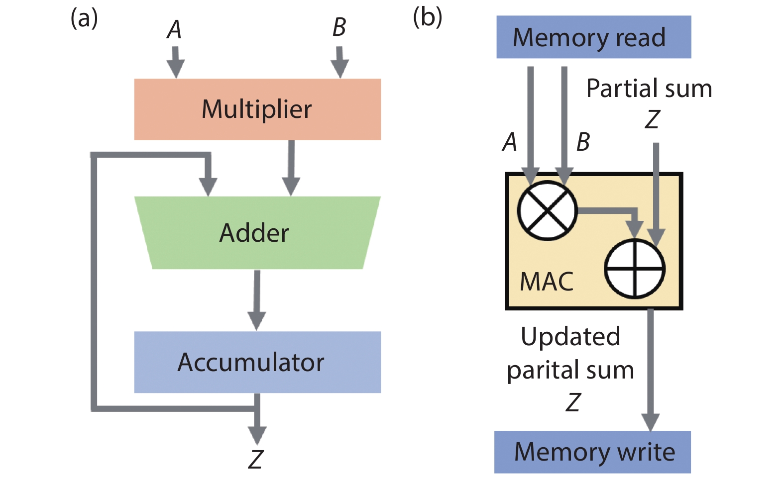
    Fig. 1. (Color online) (a) Block diagram of the basic MAC unit. (b) Memory read and write for each MAC unit.
    (Color online) One-step vector-matrix multiplication (VMM) based on memristive array during (a) forward and (b) backward processes.
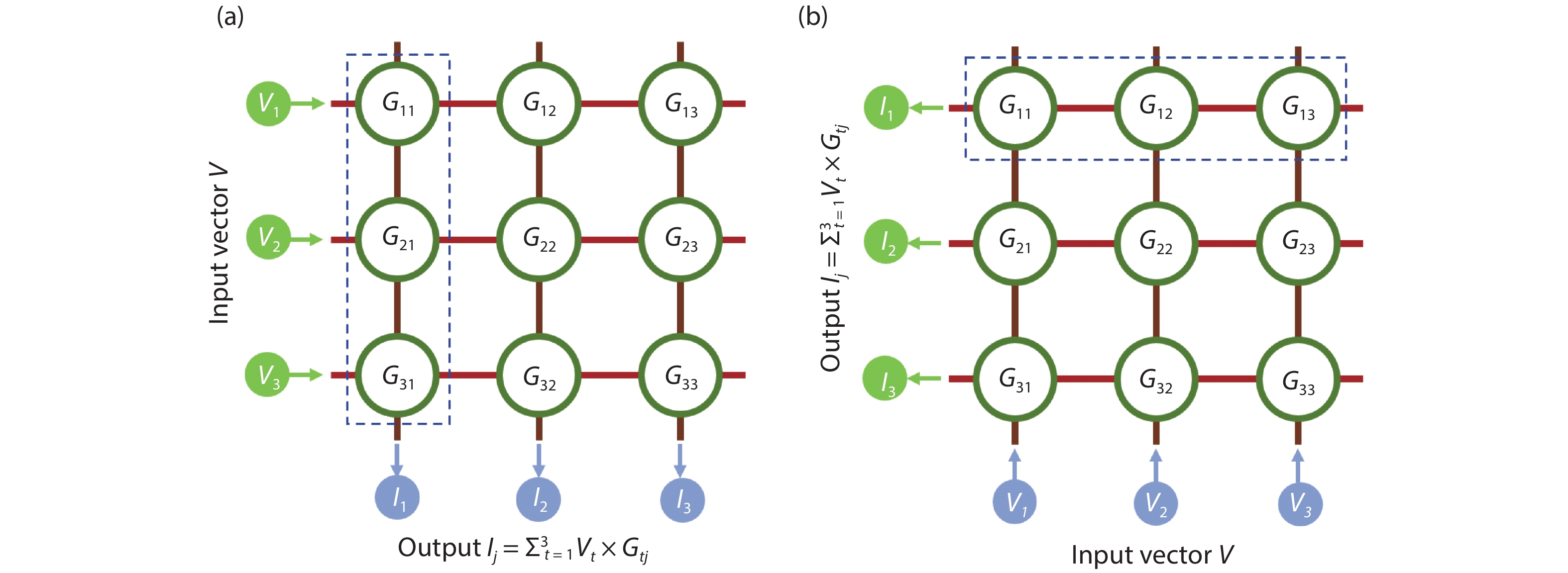
    Fig. 2. (Color online) One-step vector-matrix multiplication (VMM) based on memristive array during (a) forward and (b) backward processes.
    (Color online) Reprinted from Ref. [40]: (a) Demonstration of 128 × 64 1T1R memristor array. (b) Demonstration of accurate programming of the 1T1R memristor array with ≈180 conductance levels. And two VMM applications programmed and implemented on the DPE array: (c) a signal processing application using the discrete cosine transform (DCT) which converts a time-based signal into its frequency components, (d) a neural network application using a single-layer softmax neural network for recognition of handwritten digits.
    Fig. 3. (Color online) Reprinted from Ref. [40]: (a) Demonstration of 128 × 64 1T1R memristor array. (b) Demonstration of accurate programming of the 1T1R memristor array with ≈180 conductance levels. And two VMM applications programmed and implemented on the DPE array: (c) a signal processing application using the discrete cosine transform (DCT) which converts a time-based signal into its frequency components, (d) a neural network application using a single-layer softmax neural network for recognition of handwritten digits.
    (Color online) (a) The basic structure of a fully connected artificial neural network (ANN). In a backpropagation network, the learning algorithm has two phases: the forward propagation to compute outputs, and the back propagation to compute the back-propagated errors. (b) The mapping schematic of an ANN to memristive arrays.
    Fig. 4. (Color online) (a) The basic structure of a fully connected artificial neural network (ANN). In a backpropagation network, the learning algorithm has two phases: the forward propagation to compute outputs, and the back propagation to compute the back-propagated errors. (b) The mapping schematic of an ANN to memristive arrays.
    (Color online) Reprinted from Ref. [69]: (a) A perceptron diagram showing portions of the crossbar circuits involved in the experiment. (b) Graph representation of the implemented network. (c) Equivalent circuit for the first layer of the perceptron. Reprinted from Ref. [70]: (d) The micrograph of a fabricated 1024-cell-1T1R array using fully CMOS compatible fabrication process. (e) The schematic of parallel read operation and how a pattern is mapped to the input. Reprinted from Ref. [71]: (f) Die micrograph with SW-2T2R layout.
    Fig. 5. (Color online) Reprinted from Ref. [69]: (a) A perceptron diagram showing portions of the crossbar circuits involved in the experiment. (b) Graph representation of the implemented network. (c) Equivalent circuit for the first layer of the perceptron. Reprinted from Ref. [70]: (d) The micrograph of a fabricated 1024-cell-1T1R array using fully CMOS compatible fabrication process. (e) The schematic of parallel read operation and how a pattern is mapped to the input. Reprinted from Ref. [71]: (f) Die micrograph with SW-2T2R layout.
    (Color online) Reprinted from Ref. [74]: (a) Integrated chip wire-bonded on a pin-grid array package. (b) Cross-section schematic of the integrated chip, showing connections of the memristor array with the CMOS circuitry through extension lines and internal CMOS wiring. Inset, cross-section of the WOx device. (c) Schematic of the mixed signal interface to the 54 × 108 crossbar array, with two write DACs, one read DAC and one ADC for each row and column. Experimental demonstrations on the integrated memristor chip: (d) Single-layer perceptron using a 26 × 10 memristor subarray, (e) implementation of the LCA algorithm, (f) the bilayer network using a 9 × 2 subarray for the PCA layer and a 3 × 2 subarray for the classification layer.
    Fig. 6. (Color online) Reprinted from Ref. [74]: (a) Integrated chip wire-bonded on a pin-grid array package. (b) Cross-section schematic of the integrated chip, showing connections of the memristor array with the CMOS circuitry through extension lines and internal CMOS wiring. Inset, cross-section of the WOx device. (c) Schematic of the mixed signal interface to the 54 × 108 crossbar array, with two write DACs, one read DAC and one ADC for each row and column. Experimental demonstrations on the integrated memristor chip: (d) Single-layer perceptron using a 26 × 10 memristor subarray, (e) implementation of the LCA algorithm, (f) the bilayer network using a 9 × 2 subarray for the PCA layer and a 3 × 2 subarray for the classification layer.
    (Color online) (a) Basic structure of LeNet-5. (b) Schematic of convolution operation in an image. (c) Typical mapping method of 2D convolution to memristive arrays.
    Fig. 7. (Color online) (a) Basic structure of LeNet-5. (b) Schematic of convolution operation in an image. (c) Typical mapping method of 2D convolution to memristive arrays.
    (Color online) Reprinted from Ref. [84]: (a) The microscopic top-view image of fabricated 12 × 12 cross-point array. (b) The implementation of the Prewitt horizontal kernel (fx) and vertical kernel (fy). Reprinted from Ref. [85]: (c) Schematic of kernel operation using the two-layered 3-D structure with positive and negative weights. Reprinted from Ref. [86]: (d) The schematic of the 3D VRRAM architecture and current flow for one convolution operation. (e) The implementation of 3D Prewitt kernel Gx, Gy and Gz on 3D VRRAM.
    Fig. 8. (Color online) Reprinted from Ref. [84]: (a) The microscopic top-view image of fabricated 12 × 12 cross-point array. (b) The implementation of the Prewitt horizontal kernel (fx) and vertical kernel (fy). Reprinted from Ref. [85]: (c) Schematic of kernel operation using the two-layered 3-D structure with positive and negative weights. Reprinted from Ref. [86]: (d) The schematic of the 3D VRRAM architecture and current flow for one convolution operation. (e) The implementation of 3D Prewitt kernel Gx, Gy and Gz on 3D VRRAM.
    (Color online) Reprinted from Ref. [87]: (a) Photograph of the integrated PCB subsystem, also known as the PE board, and image of a partial PE chip consisting of a 2048-memristor array and on-chip decoder circuits. (b) Sketch of the hardware system operation flow with hybrid training used to accommodate non-ideal device characteristics for parallel memristor convolvers. Reprinted from Ref. [31]: (c) Schematic of the 3D circuits composed of high-density staircase output electrodes (blue) and pillar input electrodes (red). (d) Each kernel plane can be divided into individual row banks for a cost-effective fabrication and flexible operation. (e) Flexible row bank design enables parallel operation between pixels, filters and channels.
    Fig. 9. (Color online) Reprinted from Ref. [87]: (a) Photograph of the integrated PCB subsystem, also known as the PE board, and image of a partial PE chip consisting of a 2048-memristor array and on-chip decoder circuits. (b) Sketch of the hardware system operation flow with hybrid training used to accommodate non-ideal device characteristics for parallel memristor convolvers. Reprinted from Ref. [31]: (c) Schematic of the 3D circuits composed of high-density staircase output electrodes (blue) and pillar input electrodes (red). (d) Each kernel plane can be divided into individual row banks for a cost-effective fabrication and flexible operation. (e) Flexible row bank design enables parallel operation between pixels, filters and channels.
    (Color online) Reprinted from Ref. [88]: (a) Structure of the proposed fully CMOS-integrated 1MB 1T1R binary memristive array and on-chip peripheral circuits, comparing with previous macro based on memristive arrays and discrete off-chip peripheral circuit components (ADCs and DACs) or high-precision testing equipment. (b) MAC operations in the proposed macro. Reprinted from Ref. [89]: (c) Overview of the proposed CIM macro with multibit inputs and weights.
    Fig. 10. (Color online) Reprinted from Ref. [88]: (a) Structure of the proposed fully CMOS-integrated 1MB 1T1R binary memristive array and on-chip peripheral circuits, comparing with previous macro based on memristive arrays and discrete off-chip peripheral circuit components (ADCs and DACs) or high-precision testing equipment. (b) MAC operations in the proposed macro. Reprinted from Ref. [89]: (c) Overview of the proposed CIM macro with multibit inputs and weights.
    (Color online) Reprinted from Ref. [90]: (a) Structure of a Generative Adversarial Network (GAN). Reprinted from Ref. [92]: (b) Left panel shows the schematic of a multilayer RNN with input nodes, recurrent hidden nodes, and output nodes. Right panel is the structure of an LSTM network cell. (c) Data flow of a memristive LSTM.
    Fig. 11. (Color online) Reprinted from Ref. [90]: (a) Structure of a Generative Adversarial Network (GAN). Reprinted from Ref. [92]: (b) Left panel shows the schematic of a multilayer RNN with input nodes, recurrent hidden nodes, and output nodes. Right panel is the structure of an LSTM network cell. (c) Data flow of a memristive LSTM.
    (Color online) The application landscape for in-memory computing[10]. The applications are grouped into three main categories based on the overall degree of computational precision that is required. A qualitative measure of the computational complexity and data accesses involved in the different applications is also shown.
    Fig. 12. (Color online) The application landscape for in-memory computing[10]. The applications are grouped into three main categories based on the overall degree of computational precision that is required. A qualitative measure of the computational complexity and data accesses involved in the different applications is also shown.
    (Color online) Illustration of the hybrid in-memory computing[8]. (a) A possible architecture of a mixed-precision in-memory computing system, the high-precision unit based on von Neumann digital computer (blue part), the low precision in-memory computing unit performs analog in-memory MAC unit by one or multiple memristor arrays (red part) and the system bus (gray part) offering the overall management between two computing units. (b) Solution algorithm for the mixed-precision system to solve the linear equations , the blue boxes showing the high-precision iteration in digital unit as the red boxes presents the MAC operation in the low precision in-memory computing unit.
    Fig. 13. (Color online) Illustration of the hybrid in-memory computing[8]. (a) A possible architecture of a mixed-precision in-memory computing system, the high-precision unit based on von Neumann digital computer (blue part), the low precision in-memory computing unit performs analog in-memory MAC unit by one or multiple memristor arrays (red part) and the system bus (gray part) offering the overall management between two computing units. (b) Solution algorithm for the mixed-precision system to solve the linear equations , the blue boxes showing the high-precision iteration in digital unit as the red boxes presents the MAC operation in the low precision in-memory computing unit.
    (Color online) Reprinted from Ref. [98]: (a) A typically time-evolving 2-D partial differential system showing the change of the wave at four different time instances. (b) The sparse matrix can be used to present the differential relations between the coarse grids and can be used to solve PDEs in numerical computing. (c) Slice the sparse coefficient matrix into the same size patches and only the one contains the active elements that will be performed in the numerical computing. (d) Using multiple devices array can extend the computing precision as each array only presents the number of bits been given. (e) Mapping the elements of n-bits slices into the small memristive array as the conductance. The MAC operation will be used to accelerate the solution algorithm and the PDEs can be solved.
    Fig. 14. (Color online) Reprinted from Ref. [98]: (a) A typically time-evolving 2-D partial differential system showing the change of the wave at four different time instances. (b) The sparse matrix can be used to present the differential relations between the coarse grids and can be used to solve PDEs in numerical computing. (c) Slice the sparse coefficient matrix into the same size patches and only the one contains the active elements that will be performed in the numerical computing. (d) Using multiple devices array can extend the computing precision as each array only presents the number of bits been given. (e) Mapping the elements of n-bits slices into the small memristive array as the conductance. The MAC operation will be used to accelerate the solution algorithm and the PDEs can be solved.
    (Color online) Reprinted from Ref. [100]: (a) The in-memory computing circuit based on memristor MAC unit to solve the linear equation in one step with feedback structure. (b) The physical division of matrix inverse operation can be illustrated by the TIA, circuits to calculate a scalar productby Ohm’s law, and to calculate a scalar division by a TIA. (c) Circuits to calculate the linear equation with both positive and negative elements, the coefficient matrix A will be splinted into two positive matrix B and C which follows . (d) The circuits to calculate the eigenvector equation in one step. Another series of TIAs will be added to the circuit as the feedback conductance will mapping the known eigenvalue .
    Fig. 15. (Color online) Reprinted from Ref. [100]: (a) The in-memory computing circuit based on memristor MAC unit to solve the linear equation in one step with feedback structure. (b) The physical division of matrix inverse operation can be illustrated by the TIA, circuits to calculate a scalar product by Ohm’s law, and to calculate a scalar division by a TIA. (c) Circuits to calculate the linear equation with both positive and negative elements, the coefficient matrix A will be splinted into two positive matrix B and C which follows . (d) The circuits to calculate the eigenvector equation in one step. Another series of TIAs will be added to the circuit as the feedback conductance will mapping the known eigenvalue .
    (Color online) Emerging analog computing based on (a) phase change memory (PCM)[108]. (b) FeFET[109]. (c) NOR flash[110].
    Fig. 16. (Color online) Emerging analog computing based on (a) phase change memory (PCM)[108]. (b) FeFET[109]. (c) NOR flash[110].
    ApplicationTypeTaskEfficiencyRef.
    Memristive-based neural networksANNMNIST78.4 TOPS/W[75]
    PCA, sparse coding, recognition1.37 TOPS/W[73]
    CNNMNIST11014 GOPS/W[87
    MNIST (3D array)152.36 TOPS/W[31]
    MNIST (Binary weight)121.28 TOPS/W[90]
    LSTMPenn tree bank79 TOPS/W[97]
    GANGAN training240× performance and 94× energy saving than state-of-the-art GPU[90]
    Memristive-based scientific computing“One-shot” in-memory solverSpecialized(Eigen vector)362 TOPS/W[100]
    Mixed-precision solverGeneralized(System of linear equations)672 GOPS/W[8]
    General PDE solverSpecialized(Partial differential equations)60.1 TOPS/W[98]
    Table 1. Representative memristive-based MAC acceleration applications.
    Jia Chen, Jiancong Li, Yi Li, Xiangshui Miao. Multiply accumulate operations in memristor crossbar arrays for analog computing[J]. Journal of Semiconductors, 2021, 42(1): 013104
    Download Citation