• Journal of Semiconductors
  • Vol. 42, Issue 1, 013104 (2021)
Jia Chen1、2, Jiancong Li1、2, Yi Li1、2, and Xiangshui Miao1、2
Author Affiliations
  • 1Wuhan National Laboratory for Optoelectronics, School of Optical and Electronic Information, Huazhong University of Science and Technology, Wuhan 430074, China
  • 2Hubei Key Laboratory of Advanced Memories, Huazhong University of Science and Technology, Wuhan 430074, China
  • show less
    DOI: 10.1088/1674-4926/42/1/013104 Cite this Article
    Jia Chen, Jiancong Li, Yi Li, Xiangshui Miao. Multiply accumulate operations in memristor crossbar arrays for analog computing[J]. Journal of Semiconductors, 2021, 42(1): 013104 Copy Citation Text show less

    Abstract

    Memristors are now becoming a prominent candidate to serve as the building blocks of non-von Neumann in-memory computing architectures. By mapping analog numerical matrices into memristor crossbar arrays, efficient multiply accumulate operations can be performed in a massively parallel fashion using the physics mechanisms of Ohm’s law and Kirchhoff’s law. In this brief review, we present the recent progress in two niche applications: neural network accelerators and numerical computing units, mainly focusing on the advances in hardware demonstrations. The former one is regarded as soft computing since it can tolerant some degree of the device and array imperfections. The acceleration of multiple layer perceptrons, convolutional neural networks, generative adversarial networks, and long short-term memory neural networks are described. The latter one is hard computing because the solving of numerical problems requires high-precision devices. Several breakthroughs in memristive equation solvers with improved computation accuracies are highlighted. Besides, other nonvolatile devices with the capability of analog computing are also briefly introduced. Finally, we conclude the review with discussions on the challenges and opportunities for future research toward realizing memristive analog computing machines.

    1. Introduction

    Against the backdrop of exploding data volumes nowadays, traditional computing architectures are facing the von Neumann bottleneck[1], which has become an insurmountable technical obstacle in further enhancing the performance of computing systems. Since Moore's Law[2] has become difficult to keep going, the benefits to memory from shrinking transistor sizes are not significant, resulting in memory performance gains that are much slower than processor speed, the so-called "memory wall" that hinders performance enhancement[3-6]. In terms of raging AI chip development, AI relies on software algorithms and strong computing power in the cloud to achieve greater success, and is capable of performing a variety of specific intelligent processing tasks. But encountering many challenges such as power consumption, speed, cost, and so on, there is still a huge gap from the era of the intelligent internet of everything. As a result, in-memory computing has drawn great attention[7-15].

    In-memory computing, as the term suggests, builds the computation directly into memory, which can eliminate the large amount of data throughput that exists between the memory unit and the computing unit, significantly reducing the energy consumption generated by data migration and data access. In-memory computing shows great potential for energy saving and computing acceleration and is expected to achieve high-density, low-power, massively parallel computing systems. Meanwhile, this kind of emerging technology is still facing key challenges such as hardware resource reuse, computing-in-memory unit design, and analog computing implementation.

    As it stands, the technical paths for in-memory computing can be categorized in two ways by taking the memory as the core. One is to design circuits and architecture based on traditional memory, which is usually recognized as near-memory computing[16, 17], such as IBM's TrueNorth chip[18], Cambrian's DaDianNao chip[19], Intel’s Loihi chip[20], Tsinghua University's Tianjic chip[21], and so on. These emerging in-memory computing chips are all based on traditional SRAM or DRAM but show great improvement in energy efficiency and computing power. Strictly, the computing of traditional volatile memories is not physically performed in the memory cell. Another hugely promising scheme, on the other hand, requires the adoption of emerging non-volatile memories, including memristors[22], phase change memories[23], ferroelectric memories[24], and spintronic devices[25], etc. The non-volatile property of these emerging memories can naturally integrate the computation into memory, translating it into a weighted summation. Except digital in-memory logic implementation, these emerging devices are able to store multiple bits of analog volume in principle, which has a natural advantage in hardware implementation of in-memory analog computing. The parallel multiply accumulate (MAC) capability of memory arrays can greatly improve the computing efficiency of in-memory computing.

    As an important member of the emerging non-volatile memory, the memristor is a simple metal–insulator–metal (MIM) sandwich structure that can achieve resistance switching (from a high resistance state (HRS) to a low resistance state (LRS)) under external voltage biases. Therefore, memristors were widely used as resistive random access memory (RRAM, HRS for logic “0”, and LRS for logic “1”) in the early stage of research. In this short review, we do not discuss the developments of high-performance memristors through mechanism characterization, material, and device engineering that have been intensively studied; readers are referred to several comprehensive reviews[26-28]. In total, memristors have been evaluated in various material systems, such as metal oxides, chalcogenides, perovskites, organic materials, low-dimensional materials, and other emerging materials, which have all shown great potential in the mechanism and/or properties to improve device performances. Memristors already have strong competitiveness in terms of scalability (2-nm feature size[29]), operating speed (85 ps[30]), and integration density (8-layer 3D vertical integration[31]), etc. Since 2011, analog conductance characteristics of memristors were experimentally demonstrated to realize synaptic plasticity, the basic biological rule behind the learning and memory in the brain[32]. Under externally applied voltage excitation, the conductive filaments of the memristor, composed of oxygen vacancies or metal atoms, can be gradually grown or dissolved, allowing the memristive conductance to exhibit analog continuous increasing or decreasing in a dynamic range, rather than binary switching behaviors, which is similar to the long-term potentiation (LTP) or long-term depression (LTD) characteristics of the synapses in the brain. Since then, memristors have become one of the strong candidates of emerging analog devices for neuromorphic and in-memory computing.

    For the application of in-memory computing, analog memristors have been researched explosively and are prospected to be provided with such following properties: (1) an analog memristor essentially represents an analog quantity, which plausibly emulates biological synaptic weights, such as the implementation of LTP, LTD, and spike-timing-dependent plasticity (STDP) functions; (2) memristors have obvious performance advantages in non-volatility, simple structure, low power consumption, and high switching speed; (3) memristors are scalable and can be expanded on a large scale in terms of high-density integration, facilitating the construction of more analog computing tasks.

    In recent years, in-memory computing accelerators based on memristors have received much attention from both academia and industry. It is not just that memristor-based in-memory computing accelerators that tightly integrate analog computing and memory functions, breaking the bottleneck of data transfer between the central processor and memory in traditional von Neumann architectures. More importantly, by adding some functional units to the periphery of the memristive array, the array is able to perform MAC computing within a delay of almost one read operation without increasing with the input dimension. Meanwhile, the MAC operation is frequently used and is one of the main energy-consuming operations in various analog computing tasks, such as neural networks and equation solvers. The marriage of memristor and analog computing algorithms has given rise to a new research area, namely “memristive analog computing” or “memristive in-memory computing”.

    Notably, research and practice on this emerging interdisciplinary are still in early stages. In this paper, we conduct a comprehensive survey of the recent research efforts on memristive analog computing. This paper is organized as follows.

    (1) Section 1 reviews the background of in-memory computing and the concept of the analog memristor.

    (2) Section 2 introduces the basic MAC unit and its implementation in the memristive cross array.

    (3) Section 3 focuses on the application of memristive MAC computation in the field of neural network hardware accelerators, as a representative case of analog computing.

    (4) Section 4 mainly introduces the state-of-the-art solutions for numerical computing applications based on memristive MAC operations.

    (5) Section 5 discusses other extended memristive devices and the progress of their application in analog computing.

    (6) Finally, we discuss some open research challenges and opportunities of memristive analog computing paradigm.

    For this survey, we hope it can elicit escalating attention, stimulate fruitful discussion, and inspire further research ideas on this rapidly evolving field.

    2. Multiply accumulate (MAC) operation in analog computing

    2.1. Introduction of MAC operation

    MAC operation is an important and expensive operation, which is frequently used in digital signal processing and video/graphics applications for convolution, discrete cosine transform, Fourier transform, and so on[33-37]. The MAC performs multiplication and accumulation processes, which computes the product of two numbers and adds that product to an accumulator: Z = Z + A × B. Many basic operations, such as the dot product, matrix multiplication, digital filter operations, and even polynomial evaluation operations, can be decomposed into MAC operations, as follows:

     (1)

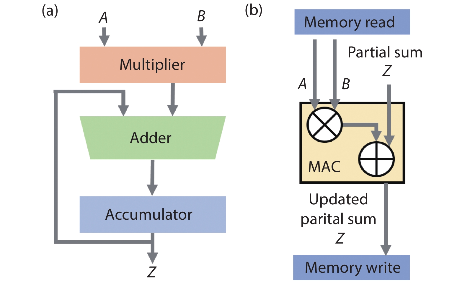
    The traditional hardware unit that performs MAC operation is known as a multiplier–accumulator (MAC unit), which is a basic computing block used extensively in general digital processors. A basic MAC unit consists of multiplier, adder, and accumulator, as shown in Fig. 1(a), which occupies a certain circuit area and consumes considerable power and delay. For read and write access to memory for each MAC unit, it needs three memory reads and one memory write as shown in Fig. 1(b). Taking a typical AlexNet network model as an example, it supports almost 724 million MACs, which means nearly 3000 million DRAM accesses will be required[38]. Therefore, any improvement in the calculation performance of the MAC unit could lead to a substantial improvement in clock speed, instruction time, and processor performance for hardware acceleration.

    (Color online) (a) Block diagram of the basic MAC unit. (b) Memory read and write for each MAC unit.

    Figure 1.(Color online) (a) Block diagram of the basic MAC unit. (b) Memory read and write for each MAC unit.

    2.2. Implementation of MAC operation in memristor array

    As a powerful alternative for improving the efficiency of data-intensive task processing in the era of big data, the in-memory computing hardware solution to the computational bottleneck is essentially a manifestation of the acceleration of MAC operations. Naturally, a memristive crossbar is highly efficient at executing vector-matrix multiplication (VMM) in one step by parallel MAC operations.

    As shown in Fig. 2, for a memristive array, each row and column crossing node represents a memristor. The numerical values in a matrix can be directly mapped as the analog conductance on the crossbar array. When a forward input vector V is applied in the form of voltage pulses with different pulse amplitudes or widths to the rows, the currents collected at the columns result from the MAC operation between the input voltages and corresponding conductance nodes, following Ohm’s law and Kirchhoff’s current law. Thus, the array implements a one-step calculation of the VMM. The same goes for backpropagation. In other words, the VMM operation could be efficiently performed with O(1) time complexity.

    (Color online) One-step vector-matrix multiplication (VMM) based on memristive array during (a) forward and (b) backward processes.

    Figure 2.(Color online) One-step vector-matrix multiplication (VMM) based on memristive array during (a) forward and (b) backward processes.

    Since VMM is an essential operation in various machine learning algorithms, in the past years developing memristor-based accelerators has become one of the mainstays of hardware neuromorphic computing. As far back as 2016, Hu et al.[39] proposed a dot-product engine (DPE) as a high density, high power efficiency accelerator for approximate VMM utilizing the natural MAC parallelism of the memristor crossbar. By inventing a conversion algorithm to map arbitrary matrix values appropriately to the memristor conductance in a realistic crossbar array, the DPE-based neural networks for pattern recognition is simulated and benchmarked with negligible accuracy degradation compared to software approach (99% recognition accuracy for the MNIST dataset). Further, experimental validations on a 128 × 64 1T1R memristor array were implemented[40, 41]. As shown in Fig. 3, two application scenarios were demonstrated on the memristive chip: a signal processing application using the discrete-cosine transform that converts a time-based signal into its frequency components, and a single-layer softmax neural network for recognition of handwritten digits with acceptable accuracy and re-programmability. Quantitatively, a > 10× computational efficiency was projected, compared to the same VMM operations performed by 40 nm CMOS digital technology with 4-bit accuracy, and a computational efficiency greater than 100 TOPs/W is possible.

    (Color online) Reprinted from Ref. [40]: (a) Demonstration of 128 × 64 1T1R memristor array. (b) Demonstration of accurate programming of the 1T1R memristor array with ≈180 conductance levels. And two VMM applications programmed and implemented on the DPE array: (c) a signal processing application using the discrete cosine transform (DCT) which converts a time-based signal into its frequency components, (d) a neural network application using a single-layer softmax neural network for recognition of handwritten digits.

    Figure 3.(Color online) Reprinted from Ref. [40]: (a) Demonstration of 128 × 64 1T1R memristor array. (b) Demonstration of accurate programming of the 1T1R memristor array with ≈180 conductance levels. And two VMM applications programmed and implemented on the DPE array: (c) a signal processing application using the discrete cosine transform (DCT) which converts a time-based signal into its frequency components, (d) a neural network application using a single-layer softmax neural network for recognition of handwritten digits.

    Hence, memristor arrays present an emerging computing platform for efficient analog computing. The ability of parallel MAC operation enables the general acceleration of any matrix operations, naturally converting into the analog domain for low-power, high-speed computation. Also, the scalability and flexibility of the array architecture make it very re-programmable and provide excellent hardware acceleration for different MAC-based applications. It is worth noting that, although the applicability of a memristor-based MAC computing system is still limited by reliability problems that arise from the immature fabrication techniques, some fault detection and error correction methods have been studied to increase technical maturity[42-44].

    3. Neural network acceleration with memristive MAC operations

    Neural networks are a sizable area for MAC-based hardware acceleration research. Widely employed in machine learning, neural networks abstract the human brain neuron network from the information processing perspective, and builds various models to form different networks according to different connections[45-48]. Deeper and more complex neural networks are needed to enhance the self-learning and data processing capabilities, and neural networks are becoming more intelligent, such as from supervised to unsupervised learning, from image processing to dynamic time-series information processing, etc. Importantly, MAC operation is always one of the most frequent computing units in various neural network models. In some published tools and methods for the evaluation and comparison of deep learning neural network chips, such as Eyeriss’s benchmarking[49], Baidu DeepBench[50], and Fathom[51], MAC/s and MAC/s/w are the important indexes to measure the overall computing performance. Thus, the highly efficient MAC operation is a major basis for the hardware acceleration of neural networks. Setting sights on the huge potential of parallel MAC computing in memristive arrays, the memristive neural networks have gotten fierce development.

    3.1. Artificial neural network (ANN)

    The fully connected multi-layer perceptron (MLP) is one of the most basic artificial neural networks (ANNs), without a biological justification. In addition to the input and output layers, it can have multiple hidden layers. The simplest two-layer MLP contains only one hidden layer and is capable of solving nonlinear function approximation problem, as shown in Fig. 3(a). For memristive neural networks, the key is the hardware mapping of the weight matrices into the memristive array, as shown in Fig. 4(b), while a large amount of MAC calculation can be executed in an efficient parallel manner for acceleration. Typically, a weight with a positive or negative value requires a differential connectio of two memristive devices: W = G+G, which means two memristive arrays are needed to load one weight matrix.

    (Color online) (a) The basic structure of a fully connected artificial neural network (ANN). In a backpropagation network, the learning algorithm has two phases: the forward propagation to compute outputs, and the back propagation to compute the back-propagated errors. (b) The mapping schematic of an ANN to memristive arrays.

    Figure 4.(Color online) (a) The basic structure of a fully connected artificial neural network (ANN). In a backpropagation network, the learning algorithm has two phases: the forward propagation to compute outputs, and the back propagation to compute the back-propagated errors. (b) The mapping schematic of an ANN to memristive arrays.

    Thanks to the capability of the memristive array to perform VMM operations in both forward and backward directions, it can naturally implement a on-chip error-backpropagation (BP) algorithm, the most successful learning algorithm. The forward pattern information and the backward error signal can both be encoded as the corresponding voltage signal input to the array, taking the MAC computing advantage to proceed with both inference and update phases of the neural network algorithm.

    In the early stages of research, many works were devoted to improving the performances of memristive devices[29, 52-57], exploring the dependence of network performance on different device properties[58-62], etc. As a result, several consensuses have also been reached on memristive ANN application:

    (1) For the multi-level analog property of memristors, 5–6 bits are generally required for basic full-precision multi-layer perceptron[63-65]. However, with adoption of the algorithm optimization of quantization, the strict requirement weight precision is lowered (4 bits or less, except binary or ternary neural networks)[66-68]. Hence, rather than pursuing continuous tuning of the device conductance, stable and distinguishable conductance states are more important for hardware implementations of memristive ANN. Moreover, reducing the lower conductance of the memristors is important for peripheral circuit design and overall system power consumption while ensuring a sufficient dynamic conductance window.

    (2) The linearity and symmetry of the bidirectional conductance tuning behavior are indeed important, both in terms of network performance and peripheral circuit friendliness. Due to the existence of device imperfections, such as read/write noises, uncontrollable dynamic conductance range, poor retention, and low array yield, the analog conductance tuning behaviors still need to be improved for better reliability. For memristor-based neural network inference engines, the accurate write-in method and the retention property of multi-level states become significant.

    (3) A simple crossbar array can cause many practical problems, including IR drop, leakage current, etc. These cannot be ignored in hardware design, especially the voltage sensing errors caused by IR drop.

    Until recently, there have been many breakthroughs in the on-chip hardware implementation of memristive ANN. As shown in Figs. 5(a)5(c), Bayat et al. demonstrated a mixed-signal integrated hardware chip for a one-hidden layer perceptron classifier with a passive 0T1R 20 × 20 memristive crossbar array[69]. The memristors in the array showed relatively low variations of I–V characteristics by counting the SET and RESET threshold, and I–V nonlinearity provided sufficient selector functionality to limit leakage currents in the crossbar circuit. Equally important, the pulse width coding method was another strategy to prove accurate read-out and weak sneak paths in this work. Off-chip and on-chip training of memristive ANN were performed for simple pixel images. This work demonstrates the excellent fabrication technology of memristive array and the great potential of memristive ANN on-chip implementation. It is worth noting that I–V nonlinearity for a passive memristive array, while helping to cut the sneak paths, also has an impact on the accurate linear read of the devices, which requires a trade-off.

    (Color online) Reprinted from Ref. [69]: (a) A perceptron diagram showing portions of the crossbar circuits involved in the experiment. (b) Graph representation of the implemented network. (c) Equivalent circuit for the first layer of the perceptron. Reprinted from Ref. [70]: (d) The micrograph of a fabricated 1024-cell-1T1R array using fully CMOS compatible fabrication process. (e) The schematic of parallel read operation and how a pattern is mapped to the input. Reprinted from Ref. [71]: (f) Die micrograph with SW-2T2R layout.

    Figure 5.(Color online) Reprinted from Ref. [69]: (a) A perceptron diagram showing portions of the crossbar circuits involved in the experiment. (b) Graph representation of the implemented network. (c) Equivalent circuit for the first layer of the perceptron. Reprinted from Ref. [70]: (d) The micrograph of a fabricated 1024-cell-1T1R array using fully CMOS compatible fabrication process. (e) The schematic of parallel read operation and how a pattern is mapped to the input. Reprinted from Ref. [71]: (f) Die micrograph with SW-2T2R layout.

    A memristive ANN chip for face recognition classification was also presented by Yao et al.[70]. As shown in Figs. 5(d) and 5(e), the chip consisted of 1024 1T1R cells with 128 rows and 8 columns and demonstrated 88.08% learning accuracy for grey-scale face images from the Yale Face Database. The transistor of 1T1R cells facilitates hardware implementation by acting as a selector, while also providing an efficient control line that allows the precise tuning of memristors. Compared with an Intel Xeon Phi processor, apart from the high recognition accuracy, this memristive ANN chip with analog weight consumed 1000 times less energy, which strongly exhibited the potential of the memristor ANN to run complex tasks with high efficiency. However, for complex applications, the coding of input information becomes an issue that cannot be ignored. The pulse width coding used in this work is obviously not a good strategy and can cause serious delays and peripheral circuitry burdens. The commonly used pulse amplitude coding, on the other hand, imposes stringent requirements on the linear conductance range of the devices[56, 72]. Recently, the same group further attempted to address two considerable challenges posed by the memristive array: the IR drop that decreases the computing accuracy and further limits the parallelism, and the inefficiency due to the power overhead of the A/D and D/A converters. By designing the sign-weighted 2T2R array and a low-power interface with resolution-adjustable LPAR-ADC, an integrated chip with 158.8 kB 2-bit memristors[73], as shown in Fig. 5(f), was implemented, which demonstrated a fully connected MLP model for MNIST recognition with high recognition accuracy (94.4%), high inference speed (77 μs/image), and 78.4 TOPS/W peak energy efficiency.

    Taking the functional completeness of the memristive ANN chips into account, a fully integrated, functional, reprogrammable memristor chip was proposed[74], including a passive memristor crossbar array directly integrated with all the necessary interface circuitry, digital buses, and an OpenRISC processor. Thanks to the re-programmability of the memristor crossbar and the integrated complementary metal–oxide–semiconductor (CMOS) circuitry, the system was highly flexible and could be programmed to implement different computing models and network structures, as shown in Fig. 6, including a perceptron network, a sparse coding algorithm, and a bilayer PCA system with an unsupervised feature extraction layer and a supervised classification layer, which allowed the prototypes to be scaled to larger systems and potentially offering efficient hardware solutions for different network sizes and applications.

    (Color online) Reprinted from Ref. [74]: (a) Integrated chip wire-bonded on a pin-grid array package. (b) Cross-section schematic of the integrated chip, showing connections of the memristor array with the CMOS circuitry through extension lines and internal CMOS wiring. Inset, cross-section of the WOx device. (c) Schematic of the mixed signal interface to the 54 × 108 crossbar array, with two write DACs, one read DAC and one ADC for each row and column. Experimental demonstrations on the integrated memristor chip: (d) Single-layer perceptron using a 26 × 10 memristor subarray, (e) implementation of the LCA algorithm, (f) the bilayer network using a 9 × 2 subarray for the PCA layer and a 3 × 2 subarray for the classification layer.

    Figure 6.(Color online) Reprinted from Ref. [74]: (a) Integrated chip wire-bonded on a pin-grid array package. (b) Cross-section schematic of the integrated chip, showing connections of the memristor array with the CMOS circuitry through extension lines and internal CMOS wiring. Inset, cross-section of the WOx device. (c) Schematic of the mixed signal interface to the 54 × 108 crossbar array, with two write DACs, one read DAC and one ADC for each row and column. Experimental demonstrations on the integrated memristor chip: (d) Single-layer perceptron using a 26 × 10 memristor subarray, (e) implementation of the LCA algorithm, (f) the bilayer network using a 9 × 2 subarray for the PCA layer and a 3 × 2 subarray for the classification layer.

    In total, from device array fabrication, core architecture design, peripheral circuit solutions, and overall system functionality improvement, the development of memristive ANN chips is maturing. With the summation property of neural networks, non-ideal factors such as the unmitigated intrinsic noise of memristor arrays will not completely constrain the development of memristive ANN chips, which suggests the adaptability of memristors to low-precision computing tasks. Based on non-volatile and natural MAC parallel properties of memristive arrays, the memristive ANN chips benefit from high integration, low power consumption, high computational parallelism, and high re-programmability, which have great promise in the field of analog computing.

    3.2. CNN/DNN

    As the amount of data information explodes, traditional fully-connected ANNs exhibit their information processing limitations. For example, there are 3 million parameters when processing a low-quality 1000 × 1000 RGB image, which is very resource-intensive. The proposal of the convolutional neural network (CNN) greatly improves this problem. The CNN performs two main features: firstly, it can effectively reduce a large amount of parameters, including simplifying the input pattern and lowering the weight volume in the network model; then, it can effectively retain the image characteristics, in line with the principles of image processing.

    CNN consists of three main parts: the convolutional layer, the pooling layer, and the fully connected layer. The convolutional layer is responsible for extracting local features in the image through the filtering of the convolutional kernel; the pooling layer is used to drastically reduce the parameter magnitude (downscaling), which not only greatly reduces the amount of computation but also effectively avoids overfitting; and the fully connected layer is similar to the part of a traditional neural network and is used to output the desired results. A typical CNN is not just a three-layer structure as mentioned above, but a multi-layer structure, such as the structure of LeNet-5 as shown in Fig. 7(a)[75]. By continuously deepening the design of the basic functional layers, deeper neural networks such as VGG[73], ResNet[76], etc. can also be implemented for more complex tasks.

    (Color online) (a) Basic structure of LeNet-5. (b) Schematic of convolution operation in an image. (c) Typical mapping method of 2D convolution to memristive arrays.

    Figure 7.(Color online) (a) Basic structure of LeNet-5. (b) Schematic of convolution operation in an image. (c) Typical mapping method of 2D convolution to memristive arrays.

    Based on the investigation of memristive ANN, memristive CNN can also be accelerated due to the parallel MAC operations, and the effect of memristive devices on CNN has similar conclusions, such as ideal linearity, symmetry, smaller variation, better retention and endurance[77-80]. However, the difference is that the CNN structure is more complex. The convolutional layer adopts a weight-sharing approach, and the connections between neurons are not fully connected, which cannot be mapped directly on a 2D memristive array. This is the primary problem that needs to be solved for the implementation of memristive CNN. Further, the characteristics of the device have different effects on the convolution layer and the fully connected layer. Generally, the convolutional layer has higher requirements for the characteristics of the device, including device variation and weight precision[67, 81-83]. Due to the cascading effect, the errors generated in the previous layer will always accumulate, causing greater disturbance to the subsequent layer. Therefore, it is further proved that for memristive CNN, the precise mapping and implementation of convolutional layers is one of the most important parts.

    As shown in Fig. 7(b), it is the basic principle of the image convolution operation. By sliding the convolution kernels over the image, the pixel value of the image is multiplied by the value on the corresponding convolution kernels, and then all the multiplied values are added as the grayscale value of the corresponding pixel point in the feature map until the entire convolution process is done. The most commonly used mapping method on memristive arrays is to store the weights of the convolutional kernels in the array. Specifically, as shown in Fig. 7(c), a column of the memristive array is used to store a convolutional kernel, the two-dimensional image is unrolled as a one-dimensional input voltage signal, and the information of the convolutional feature image is obtained as the output current value of the array.

    As shown in Fig. 8(a), Gao et al. firstly implemented convolution operation on a 12 × 12 memristor crossbar array in 2016[84]. Prewitt kernels were used as a proof-of-concept demonstration to detect horizontal and vertical edges of the MNIST handwritten digits. Huang et al. have also attempted to implement convolutional operations in three-dimensional memristive arrays with a Laplace kernel for edge detection of images (Fig. 8(b))[85]. More recently, Huo et al. preliminary validated 3D convolution operations on a HfO2/TaOx-based eight-layer 3D VRRAM to pave the way for 3D CNNs (Fig. 8(c))[86].

    (Color online) Reprinted from Ref. [84]: (a) The microscopic top-view image of fabricated 12 × 12 cross-point array. (b) The implementation of the Prewitt horizontal kernel (fx) and vertical kernel (fy). Reprinted from Ref. [85]: (c) Schematic of kernel operation using the two-layered 3-D structure with positive and negative weights. Reprinted from Ref. [86]: (d) The schematic of the 3D VRRAM architecture and current flow for one convolution operation. (e) The implementation of 3D Prewitt kernel Gx, Gy and Gz on 3D VRRAM.

    Figure 8.(Color online) Reprinted from Ref. [84]: (a) The microscopic top-view image of fabricated 12 × 12 cross-point array. (b) The implementation of the Prewitt horizontal kernel (fx) and vertical kernel (fy). Reprinted from Ref. [85]: (c) Schematic of kernel operation using the two-layered 3-D structure with positive and negative weights. Reprinted from Ref. [86]: (d) The schematic of the 3D VRRAM architecture and current flow for one convolution operation. (e) The implementation of 3D Prewitt kernel Gx, Gy and Gz on 3D VRRAM.

    Although the preliminary implementation of convolution operation on 2D and 3D memristive arrays has been achieved, this mapping approach still has significant concerns. First, the conversion of a 2D matrix to 1D vectors losses the structural information of the image, which is still important in the subsequent process, and also causes very complex data processing in the back-propagation process. Secondly, if the one-shot MAC operation of one-dimensional image information is required for convolution, the memristive array is sparsely stored for convolution kernels, and too many unused cells could cause serious sneak path issues. While compact kernels on arrays without any redundancy space require more complex rearrangements of the input image and sacrifice significant time delays and peripheral circuits for convolution operation. In one word, the problem of convolutional operation raises challenges that need to be properly addressed while training memristive CNNs.

    Recently, to solve the severe speed mismatch between the memristive fully connected layer and convolutional layer, which comes from the time consumption during the sliding process, Yao et al. proposed a promising way of replicating the same group of weights in multiple parallel memristor arrays to recognize an input image efficiently in a memristive CNN chip[87]. A five-layer CNN with three duplicated parallel convolvers on the eight memristor PEs was successfully established in a fully hardware system, as shown in Figs. 9(a) and 9(b), which allowed the processing of three data batches at the same time for further acceleration. Moreover, a hybrid training method was designed to circumvent non-ideal device characteristics. After ex-situ training and close-loop writing, only the last fully connected layer was trained in situ to tune the device conductance. In this way, not only the existing device imperfections could be compensated, but also the complex on-chip operations of backpropagation process for convolutional layers were eliminated. Hence, the performance benchmark of the memristor-based CNN system showed 110 times better energy efficiency (11 014 GOP s−1 W−1) and 30 times better performance density (1164 GOP s−1 mm−2) compared with Tesla V100 GPU, which also suffered a rather low accuracy loss (2.92% compared to software testing result) for MNIST recognition. However, in practice, transferring the same weights to multiple parallel memristor convolvers calls for high uniformity of different memristive arrays, otherwise it would induce unavoidable and random mapping error to hamper the system performance. Besides, the interconnection among memristor PEs could consume a lot of peripheral circuitry.

    (Color online) Reprinted from Ref. [87]: (a) Photograph of the integrated PCB subsystem, also known as the PE board, and image of a partial PE chip consisting of a 2048-memristor array and on-chip decoder circuits. (b) Sketch of the hardware system operation flow with hybrid training used to accommodate non-ideal device characteristics for parallel memristor convolvers. Reprinted from Ref. [31]: (c) Schematic of the 3D circuits composed of high-density staircase output electrodes (blue) and pillar input electrodes (red). (d) Each kernel plane can be divided into individual row banks for a cost-effective fabrication and flexible operation. (e) Flexible row bank design enables parallel operation between pixels, filters and channels.

    Figure 9.(Color online) Reprinted from Ref. [87]: (a) Photograph of the integrated PCB subsystem, also known as the PE board, and image of a partial PE chip consisting of a 2048-memristor array and on-chip decoder circuits. (b) Sketch of the hardware system operation flow with hybrid training used to accommodate non-ideal device characteristics for parallel memristor convolvers. Reprinted from Ref. [31]: (c) Schematic of the 3D circuits composed of high-density staircase output electrodes (blue) and pillar input electrodes (red). (d) Each kernel plane can be divided into individual row banks for a cost-effective fabrication and flexible operation. (e) Flexible row bank design enables parallel operation between pixels, filters and channels.

    A more recent work by Lin et al. has demonstrated a unique 3D memristive array to break through the limitations of 2D arrays that can only accomplish simplified interconnections[31]. As shown in Figs. 9(c)9(e), the unique 3D topology is implemented by a non-orthogonal alignment between the input pillar electrodes and output staircase electrodes that form dense but localized connections, and different 3D row banks are physically isolated from each other. And thanks to locally connected structure, it can be extended horizontally with high sensing accuracy and high voltage delivery efficiency, independent of the array issues such as sneak path and IR drop. By dividing the convolution kernels into different row banks, pixel-wise parallel convolutions could be implemented with high compactness and efficiency. The 3D design handles the spatial and temporal nature of convolution so that the feature maps can be directly obtained at the output of the array with a minimal amount of post-processing. For complex neural networks, the row banks are highly scalable and independent so that they can be flexibly programmed for different output pixels, filters, or kernels from different convolutional layers, which offers substantial benefits in simplifying and shortening the massive and complex connections between convolutional layers. Such a customized three-dimensional memristor array design is a critical avenue towards the CNN accelerator with more complex function and higher computation efficiency.

    It can be seen that to improve the efficiency of a memristive CNN, various mapping methods for memristive arrays are being actively explored, including multiplex and interconnection of multiple small two-dimensional arrays, or specially designed 3D stacking structures. In addition to considering the mapping design of the memristive array cores, the peripheral circuit implementation of memristive CNN is another important concern, which also determines the performance and efficiency of the system to a large extent. While memristive arrays are conducive to efficient analog computing, the consumed ADCs and DACs come at a cost. Moreover, due to the severe resistive drift, the accurate readout circuit is also worthy of further investigation.

    Chang et al. have placed their effort on circuit optimization for on-chip memristive neural networks. They proposed an approach of efficient logic and MAC operation on their fabricated 1Mb 1T1R binary memristive array. As shown in Figs. 10(a) and 10(b), the structure of the fully integrated memristive macro included a 1T1R memristor array, digital dual-mode word line (WL) drivers (D-WLDRs), small-offset multi-level current-mode sense amplifiers (ML-CSAs), and a mode-and-input-aware reference current generator (MIA-RCG). Specifically, D-WLDRs, which replaced DACs, were used to control the gates of the NMOS transistors of 1T1R cells sharing the same row. Two read-out circuit techniques (ML-CSAs and MIA-RCG) were designed. Thus, high area overhead, power consumption, and long latency caused by high-precision ADCs could be eliminated; reliable MAC operations for the small sensing margin caused by device variability and pattern-dependent current leakage could be enhanced. Based on such circuit optimization, a 1-MB memristor-based CIM macro with 2-bit inputs and 3-bit weights for CNN-based AI edge processors was further developed[89], which overcame an area-latency-energy trade-off for multibit MAC operations, pattern dependent degradation in the signal margin, and small read margin. These system-level trials verified that high accuracy and high energy-efficiency could be achieved using a fully CMOS-integrated memristive macro for CNN. However, in general, the input information and weight precision are much more complex, at which point the design and optimization of peripheral circuits becomes a more problematic issue, and must be addressed when the memristive CNN goes deeper.

    (Color online) Reprinted from Ref. [88]: (a) Structure of the proposed fully CMOS-integrated 1MB 1T1R binary memristive array and on-chip peripheral circuits, comparing with previous macro based on memristive arrays and discrete off-chip peripheral circuit components (ADCs and DACs) or high-precision testing equipment. (b) MAC operations in the proposed macro. Reprinted from Ref. [89]: (c) Overview of the proposed CIM macro with multibit inputs and weights.

    Figure 10.(Color online) Reprinted from Ref. [88]: (a) Structure of the proposed fully CMOS-integrated 1MB 1T1R binary memristive array and on-chip peripheral circuits, comparing with previous macro based on memristive arrays and discrete off-chip peripheral circuit components (ADCs and DACs) or high-precision testing equipment. (b) MAC operations in the proposed macro. Reprinted from Ref. [89]: (c) Overview of the proposed CIM macro with multibit inputs and weights.

    3.3. Other network models

    Based on the parallel MAC computing in an array, more memristive neural network models have been investigated. One example is the generative adversarial network (GAN), which is a kind of unsupervised learning by having two neural networks play against each other to learn itself. GAN has two subnetworks: a discriminator (D) and a generator (G), as illustrated in Fig. 11(a). Both D and G typically are modeled as deep neural networks. In general, D is a classifier that is trained by distinguishing real samples from generated ones and G is optimized to produce samples that can fool the discriminator. On the one hand, two competing networks are simultaneously co-trained, which significantly increases the need for memory and computation resources. To address this issue, Chen et al proposed ReGAN, a memristor-based accelerator for GAN training, which achieved 240× performance speedup compared to GPU platform averagely, with an average energy saving of 94×[90]. On the other hand, GAN suffers from mode dropping and gradient vanishing issues, but adding continuous random noise externally to the inputs of the discriminator is very important and helpful, which takes advantage of the non-ideal effects of memristors. Thus, Lin et al. experimentally demonstrated a GAN based on a 1 kB analog memristor array to generate a different pattern of digital numbers[91]. The intrinsic random noises of analog memristors were utilized as the input of the neural network to improve the diversity of the generated numbers.

    (Color online) Reprinted from Ref. [90]: (a) Structure of a Generative Adversarial Network (GAN). Reprinted from Ref. [92]: (b) Left panel shows the schematic of a multilayer RNN with input nodes, recurrent hidden nodes, and output nodes. Right panel is the structure of an LSTM network cell. (c) Data flow of a memristive LSTM.

    Figure 11.(Color online) Reprinted from Ref. [90]: (a) Structure of a Generative Adversarial Network (GAN). Reprinted from Ref. [92]: (b) Left panel shows the schematic of a multilayer RNN with input nodes, recurrent hidden nodes, and output nodes. Right panel is the structure of an LSTM network cell. (c) Data flow of a memristive LSTM.

    Another example is the long short-term memory (LSTM) neural network, which is a special kind of recurrent neural network. LSTM is proposed to solve the "gradient disappearance" problem, and is suitable for processing and predicting events with relatively long intervals and delays in a time series. By connecting a fully connected network to a LSTM network, a two-layer LSTM network is illustrated in Fig. 11(b). Traditional LSTM cells consist of a memory cell to store state information and three gate layers that control flow of information within cells and network. The LSTM network with significantly increased complexity and a large number of parameters have a bottleneck in computing power resulting from both limited memory capacity and bandwidth. Hence, besides the implementation of the fully connected layer, memristive LSTM pays more attention to store a large number of parameters and offer in-memory computing capability for the LSTM layer, as shown in Fig. 11(c). Memristive LSTMs have been demonstrated for gait recognition, text prediction, and so on[92-97]. Experimentally, on-chip evaluations were performed on a 2.5M analog phase change memory (PCM) array and a 128 × 64 1T1R memristor array, which have also proved strongly that the memristive LSTM platform would be a promising low-power and low-latency hardware implementation.

    4. Memristor-based MAC for numerical computing

    In previous sections, we introduced the acceleration of various neural networks by using MAC operations with low computation complexity in arrays. As shown in Fig. 12, in general, these neuromorphic computing and deep learning tasks can be considered to be “soft” computations[98], as they have a high tolerance for low precision results without significant performance degradation. In contrast, scientific computing applications, which also include a large number of MAC-intensive numerical calculations, have very stringent requirements for computation precision and are thus considered as “hard” computing[10]. Numerical computing means solving accurate numerical solutions of linear algebra, partial differential equations (PDEs), and regression problems, etc., which can hardly be effectively accelerated if there are severe inter-device and intra-device variations and other device non-ideal factors.

    (Color online) The application landscape for in-memory computing[10]. The applications are grouped into three main categories based on the overall degree of computational precision that is required. A qualitative measure of the computational complexity and data accesses involved in the different applications is also shown.

    Figure 12.(Color online) The application landscape for in-memory computing[10]. The applications are grouped into three main categories based on the overall degree of computational precision that is required. A qualitative measure of the computational complexity and data accesses involved in the different applications is also shown.

    To date, the accuracy of analog MAC operation in a memristor array is still relatively limited, so building an accelerator suitable for numerical computation, as an interesting topic, remains a great challenge and, again, an excellent opportunity to further develop potential application scenarios for memristive in-memory computing. In view of this, in recent years, some remarkable technological solutions have been proposed, achieving new breakthroughs from principle to verification.

    4.1. Mixed-precision architecture

    Typically, to reach the numerical accuracy usually required for a digital computer to execute the data analytics and scientific computing. For the memristor-based MAC processer, the limitations arising from the device non-ideal factors must be addressed.

    Le Gallo et al. introduced a mixed-precision in-memory computing architecture, to process the numerical computing tasks[8]. By combing the memristor-based MAC unit with the von Neumann machine, the mixed-precision system can benefit from both the energy/area efficiency of the in-memory processing unit and the high precision computing ability of the digital computer.

    In this hybrid system, the memristor process unit performs the bulk of MAC operations, as the digital computer implements a backward method to improve the calculation accuracy and provides other mathematical operations like iteration (Fig. 13(a)). To illustrate the concept, the process of solving linear equations was shown.

    (Color online) Illustration of the hybrid in-memory computing[8]. (a) A possible architecture of a mixed-precision in-memory computing system, the high-precision unit based on von Neumann digital computer (blue part), the low precision in-memory computing unit performs analog in-memory MAC unit by one or multiple memristor arrays (red part) and the system bus (gray part) offering the overall management between two computing units. (b) Solution algorithm for the mixed-precision system to solve the linear equations , the blue boxes showing the high-precision iteration in digital unit as the red boxes presents the MAC operation in the low precision in-memory computing unit.

    Figure 13.(Color online) Illustration of the hybrid in-memory computing[8]. (a) A possible architecture of a mixed-precision in-memory computing system, the high-precision unit based on von Neumann digital computer (blue part), the low precision in-memory computing unit performs analog in-memory MAC unit by one or multiple memristor arrays (red part) and the system bus (gray part) offering the overall management between two computing units. (b) Solution algorithm for the mixed-precision system to solve the linear equations , the blue boxes showing the high-precision iteration in digital unit as the red boxes presents the MAC operation in the low precision in-memory computing unit.

    Solving the linear equations is to find an unknown vector to satisfy the constraint condition:

     (2)

    The matrix A is known as the coefficient matrix and is a non-singular matrix, the b is also known as a column vector.

    An iterative refinement algorithm was utilized in the mixed precision architecture. An initial solution was chosen as the start point, and the solving algorithm iteratively updated with a low precision error-correction term z by solving the equation in the inexact inner solver with the used as the residual. The solving algorithm ran until the residual was below the designed tolerance, and the krylov-subspace iterations method was used to solve the equation in the inexact inner solver (Fig. 13(b)).

    Experimentally, a prototype memristive MAC chip containing one million phase-change memory (PCM) array, which consists of 512 world lines and 2048 bit lines, was used to construct the low precision computing unit. Since the current is a non-linear function in the PCM, a ‘pseudo’ Ohm’s law was employed in the MAC operation:

     (3)

    The is an adjustable parameter and by approximating the I–V characteristics of the PCM device, the function can be obtained. An iterative and program-verify procedure was adopted to program the conductance to the target value .

    As the main application of this work was to solve the dense covariance matrix problems, a practical problem in which the coefficient matrix A is based on real-world RNA data was used to test the mixed-precision computer. By using the iterative refinement method and the ‘pseudo’ Ohm’s law, the mixed-precision computer is capable of solving a linear system with 5000 equations, the achievable speedup comes from reducing the number of iterations need to solve the problems and result in overall computational complexity of O(N2) for an N × N matrix, which is usually O(N3) in traditional numerical algorithms.

    Moreover, the energy efficiency of the mixed-precision computer has been further estimated by the research team. The energy efficiency of a fully integrated mixed-precision computer is 24 times higher than the state-of-the-art CPU/GPU to deal with 64-bit precision problems. Their results also show that the PCM chip offers up to 80 times lower energy consumption than the field-programmable gate array (FPGA) when dealing with low-precision 4-bit MAC operations.

    As this mixed-precision computer can outperform the traditional von Neumann computer in terms of energy consumption and processing speed. How to extend this architecture and method of solving linear equations to more applications such as optimization problem, deep learning, signal processing, automatic control, etc. in the future deserves further in-depth study.

    4.2. Matrix slice and bit slice

    The mixed-precision in-memory computing has been verified to be able to improve the MAC calculating accuracy, but the scale of the matrix that can be processed by the MAC unit is still limited by the scale of the memristive array. Moreover, as the array size increases, the impact of intra-device variation and other problems such as the I-R drop will come to the fore.

    Zidan et al. recently introduced a high-precision general memristor based partial differential equation (PDE) solver, in which multiply small memristive arrays were used to solve both the static and time-evolving partial differential equations[98].

    As the partial differential systems usually contain hyper dimensional matrices, especially for high-precision solution. For example, a 2-D partial system that is divided to 100 × 100 coarse grids can lead to a coefficient matrix with elements (Fig. 14(a)). More importantly, the coefficient matrices of the partial systems are typically sparse matrixes (Fig. 14(b)). That makes it difficult and inefficient to map the whole partial differential coefficient matrix into a single array. Fortunately, by taking advantage of sparsity, the partial coefficient matrix can be divided into equally sized slices (Fig. 14(c)). Hence, multiple small-sized arrays can be used to map the slices that contain the active elements (the non-zero elements). Besides, since all the devices will be selected during the MAC operation, the influence of the device non-linearity is trivial in the small array, and parasitic effects due to series resistance, sneak currents and imperfect virtual grounds will also be minimized. Moreover, using multiple arrays can also extend the low-native precision of the memristive devices as each array only presents the given number of bits (Fig. 14(d)). This precision expansion approach is similar to the bit-slice techniques used in the high precision digital computers. Assuming that a memristor can natively support a number l of resistance levels, the goal is thus to perform high precision arithmetic operations using base- numbers, imitating the use of base-2 numbers in digital computers.

    (Color online) Reprinted from Ref. [98]: (a) A typically time-evolving 2-D partial differential system showing the change of the wave at four different time instances. (b) The sparse matrix can be used to present the differential relations between the coarse grids and can be used to solve PDEs in numerical computing. (c) Slice the sparse coefficient matrix into the same size patches and only the one contains the active elements that will be performed in the numerical computing. (d) Using multiple devices array can extend the computing precision as each array only presents the number of bits been given. (e) Mapping the elements of n-bits slices into the small memristive array as the conductance. The MAC operation will be used to accelerate the solution algorithm and the PDEs can be solved.

    Figure 14.(Color online) Reprinted from Ref. [98]: (a) A typically time-evolving 2-D partial differential system showing the change of the wave at four different time instances. (b) The sparse matrix can be used to present the differential relations between the coarse grids and can be used to solve PDEs in numerical computing. (c) Slice the sparse coefficient matrix into the same size patches and only the one contains the active elements that will be performed in the numerical computing. (d) Using multiple devices array can extend the computing precision as each array only presents the number of bits been given. (e) Mapping the elements of n-bits slices into the small memristive array as the conductance. The MAC operation will be used to accelerate the solution algorithm and the PDEs can be solved.

    A complete hardware platform and software package were implemented for the experimental test. Ta2O5–x memristor arrays were integrated on a printed circuit board (PCB) to store the partial differential coefficient matrix and execute the MAC operation. The Python software package provided the system level operations including matrix slices, high-precision matrix mapping, and the iteration process control. The software package also presented the interface between the hardware and end user for data input/output. To test the performance of the general solver, a Poisson’s equation and a 2-D wave equation were used as the static and time-evolving solution examples. Besides, the PDE solver was inserted into the workflow of a plasma-hydrodynamics simulator to verify its applicability. Benefiting from the architecture-level optimizations such as the precision-extension techniques, the PDE solver can perform computations achieving 64-bit accuracy.

    The introduction of the matrix and bit slice technique can also substantially improve the energy efficiency of the in-memory MAC unit to execute sparse matrix computation. The energy efficiency of a 64-bit fully integrated memristor matrix slice system was reported to have achieved 950 GOPs/W, whereas the energy efficiency of the state-of-art CPU and GPU to process a sparse matrix with the same accuracy requirement is 0.3 GOPs/W (Intel Xeon Phi 7250) and 0.45 GOPs/W (NVIDIA Tesla V100)[98]. When executing an 8-bit sparse operation, the energy efficiency of this fully integrated system is 60.1 TOPs/W, while the energy efficiency of the Google TPU when performing the same operation is 2.3 TOPs/W[99].

    Note that the matrix slice method can only be used for systems with sparse coefficient matrix with limitation in reconfigurability. Although the bit-slice technique already shows the ability to improve the accuracy of the analogue MAC operation, to control multiple crossbar arrays will increase the system complexity.

    4.3. One-shot operation for numerical computing

    To further reduce the dependence on the von Neumann computer or software package. Sun et.al recently demonstrated a pure in-memory computing circuit based on the memristor MAC unit to process linear algebra problems. With a feedback structure, the computing circuit has the ability to implement solving linear equation in the so-called “one-shot operation” and O(1) time complexity can be achieved[100]. With the high energy/area efficiency and high process speed, this one-shot computing circuit can be used to solve the Schrödinger equation and accelerate those classic numerical algorithms like the PageRank algorithm[101].

    Basically, solving linear equations usually requires a large number of iterations in the mathematical solution algorithms. The in-memory solver based on the numerical algorithms will also be suffering from the performance degradation due to the data transfer between the digital processing unit and in-memory processing unit during the iterative cycles. The “one-shot” solvers, on the construct, based on the inevitability of coefficient matrix A and motivated by the circuit principles, can eliminate the limitation of the numerical iteration.

    Fig. 15(a) clearly illustrated this proposed in-memory computing circuit. The array performed the MAC operation . The operational amplifiers (OAs) were connected to the memristive array to construct the transimpedance amplifiers (TIAs). These TIAs performed the inverse operation (Fig. 15(b)). For linear equations with non-singular coefficient matrix , the solution could be written as . This solution form satisfied the output of TIAs and became the basis to solve linear equations in a one-shot operation.

    (Color online) Reprinted from Ref. [100]: (a) The in-memory computing circuit based on memristor MAC unit to solve the linear equation in one step with feedback structure. (b) The physical division of matrix inverse operation can be illustrated by the TIA, circuits to calculate a scalar productby Ohm’s law, and to calculate a scalar division by a TIA. (c) Circuits to calculate the linear equation with both positive and negative elements, the coefficient matrix A will be splinted into two positive matrix B and C which follows . (d) The circuits to calculate the eigenvector equation in one step. Another series of TIAs will be added to the circuit as the feedback conductance will mapping the known eigenvalue .

    Figure 15.(Color online) Reprinted from Ref. [100]: (a) The in-memory computing circuit based on memristor MAC unit to solve the linear equation in one step with feedback structure. (b) The physical division of matrix inverse operation can be illustrated by the TIA, circuits to calculate a scalar product by Ohm’s law, and to calculate a scalar division by a TIA. (c) Circuits to calculate the linear equation with both positive and negative elements, the coefficient matrix A will be splinted into two positive matrix B and C which follows . (d) The circuits to calculate the eigenvector equation in one step. Another series of TIAs will be added to the circuit as the feedback conductance will mapping the known eigenvalue .

    Thus, to solve the linear equations in this proposed in-memory computing circuit, the target vector is converted to the current vector and be used as the input of the circuit. And the coefficient matrix A is mapped to the device conductance matrix . The solution vector is represented by the output voltage vector under the action of Ohm’s law and Kirchhoff current law.

    As device conductance can only map positive elements, to solve equations with both positive and negative elements, another memristive array was connected to the circuit with the inverting amplifiers (Fig. 15(c)). The coefficient matrix A was splinted into two positive matrices, B and C. The matrix was implemented by . The circuit input was also constructed by and the linear equations with negative elements could be solved.

    Eigenvector calculation could also be implemented in the one-step operation. To solve the eigenvector equation , another series of TIAs were added to the circuits with the feedback resistors (Fig. 15(d)). The eigenvalue was mapped to the resistance value . Based on the circuit principles, the output of the eigenvector circuit could be written as , which satisfied the solution of the eigenvector equation.

    A 3 × 3 Ti/HfO2/C memristive array was experimentally used to construct these one-shot computing circuits. The real-world data was also used to test the performance of the circuits, a 100 × 100 memristive array based on a memristive device model was constructed for simulation to solve the 1-D steady-state Fourier equation. This partial differential equation was converted to a linear form by the finite difference method. A 1-D time-independent Schrödinger equation also was solved in the simulation with the same scale memristive array to test the performance of the eigenvector solution. Moreover, the eigenvector computing circuit can accelerate the PageRank algorithm with significant improvements in speed and energy efficiency for practical big-data tasks, such as the Havard 500 data set.

    Based on the feedback amplifiers theory and the circuit dynamics, further analysis results showed that only if the minimal eigenvalue (or real part of eigenvalue) of the coefficient matrix is positive, the system of the linear equations can be solved by the circuit in Fig. 15(a). The computation time is free of the N-dependence, rather determined solely by . The time complexity of solving model covariance matrices is O(1). The computation time of the eigenvector solution circuit also shows no dependence on the matrix size N, and relies solely on the mismatch degree of eigenvalue implementation in the circuit. Thus, the time complexity of the eigenvector direct solver is also O(1)[102-104].

    As the computing time is free of the N-dependence, the “one-shot solver” can significantly boost the computing performance and realize high energy efficiency, especially in the scene of processing data-intensive tasks. Take the eigenvector solution circuit as an example, its energy efficiency achieves 362 TOPs/W when running the PageRank algorithm for a 500 × 500 coefficient matrix. Compared to the energy efficiency of 2.3 TOPS/W of the tensor processing unit (TPU), the in-memory direct solver provides 157 times better performance.

    Although these “one-shot” circuits require a high-performance device to improve the computing accuracy, this work shows great potential to process numerical problems with high process speed (O(1) time-complexity) and low energy consumption. This circuit is particularly suited to those scenarios that require high process speed and low energy consumption but low precision. However, as the implementation of the one-shot computing circuit is hardwired, the scalability of these computing circuits should be further improved.

    4.4. Short conclusion

    Although the approximate solutions are sufficient for many computing tasks in the domain of machine learning, the numerical computing tasks, especially the scientific computing tasks pose high requirement on high precision numerical results. To evaluate the overall performance of an in-memory system for numerical computing, the system complexity, computational time complexity, computing accuracy, and energy/area efficiency need to be considered in a comprehensive manner.

    Taking advantage of sparsity, the matrix slice processor has shown a good potential to process a giant sparse matrix by using multiply small-scale arrays with high processing speed and low energy consumption. Combining this with the traditional bit-slice technique, a high precision solution can be obtained. This technique can also be used to expand the application of the traditional flash memory to process numerical missions[105]. However, the inaccuracy arising from the analogue summation still remains as the matrix scale becomes larger. Besides, bit-slicing and matrix slicing operations require additional peripheral circuitry and thus reduces the integration density of the computing system.

    By combining a von Neumann machine with the memristive MAC unit, the mixed-precision in-memory computing architecture already overperforms the CPU/GPU-based numerical computers in terms of the energy consumption and computation speed, with the same accuracy level to process giant non-sparse matrices. The mixed-precision system still suffers from the fact that the data needs to be stored both in the memristor array and the high-precision digital unit. Additional resources are needed to solve the problem. Although O(N2) computation time complexity can be achieved, it still depends on the matrix scale.

    With the fastest process speed and highest energy/area efficiency, the one-shot in-memory computing architecture is another good example of the powerful capability of the memristive MAC unit, and can even outperform the quantum computing accelerator in computation complexity[106]. This architecture can also satisfy the approximate solution for machine learning problems such as the linear regression and logic regression problems[107]. However, the one-shot computing requires a high performance memristive device with precise conductance programming and high IV linearity. Moreover, the hardwired circuits at this stage limits the system reconfigurability.

    For further development of the memristor-based numerical computation system, the first issue is to improve the programming precision of the memristors. Besides, at the algorithmic level, how a range of important numerical algorithms such as matrix factorization can be implemented efficiently in a memristive MAC unit remains a challenge. These recent breakthroughs mainly focused on the non-singular linear equations, we believe the solution of singular linear equations, non-linearity equations, and ordinary differential equations, etc. also deserve attention. After that, we can envisage the construction of a universal equation solver and even develop it to a universal numerical processor.

    5. MAC operation in other nonvolatile devices

    As one of the representatives of the emerging non-volatile devices, the memristor, based on the analog property and the parallel MAC computing, demonstrates the hardware acceleration in different fields, from low-precision neural networks to numerical analysis with high precision requirements. Since the core idea is to store and update nonvolatile conductance states in a high-density nano-array, it is naturally easy to think that other nonvolatile devices could be used to perform similar functions, although based on different physical mechanisms.

    In past decades, many other types of non-volatile devices, such as phase change memory (PCM), magnetic tunneling junctions, ferroelectric field effect transistors (FeFETs), and floating gate transistors have been intensively studied for high-performance memory application. Recently, many studies have proved that these devices can perform MAC operations and thus accelerate computing.

    Phase change memory (PCM) works by the transformations of the crystalline phase (LRS) and amorphous phase (HRS) of the chalcogenide material as its basic principle. The RESET process of PCM is relatively abrupt due to the melting and rapid cooling of the crystalline, and the naturally asymmetric conductance tuning leads to a more complex synaptic unit. To realize the bi-directional analog conductance modulation as a synaptic device, generally, two PCMs are seen as one synaptic unit, while only the analog SET process is used to implement the LTP or LTD process[111, 112]. By this method, Burr et al. experimentally demonstrated a three-layer neural network based on 164 885 PCM synapses, while the 2-PCM units showed a symmetric, linear conductance response with a high dynamic range[113]. Further, a ‘2PCM + 3T1C’ unit cell was proposed with both more dynamic range and better update symmetry[108], thus making software-equivalent training accuracies for MNIST, CIFAR-10, and even CIFAR-100 by a simulated MLP model (Fig. 16(a)). However, such PCM-based functional units are relatively area cost, greatly lowering the integration density. Furthermore, thermal management, resistance drift, and high RESET current for PCM have to be properly solved in practical applications[114, 115].

    (Color online) Emerging analog computing based on (a) phase change memory (PCM)[108]. (b) FeFET[109]. (c) NOR flash[110].

    Figure 16.(Color online) Emerging analog computing based on (a) phase change memory (PCM)[108]. (b) FeFET[109]. (c) NOR flash[110].

    Ferroelectric devices tune the device resistance by reversibly switching between the two remnant polarized states. FeFET is a three-terminal device and uses a ferroelectric thin film as the gate insulator, which is highly compatible with the CMOS process. The multi-domain polarization switching capability of a polycrystalline ferroelectric thin film can be utilized to modulate FeFET channel conductance, thus the multi-conductance levels can be used in analog computing[64, 116, 117]. Jerry et al. demonstrated a FeFET-based synaptic device using Hf0.5Zr0.5O2 (HZO) as the ferroelectric material[109]. By adjusting the applied voltages, the LTP and LTD curves of FeFET exhibited excellent linearity and symmetry, as shown in Fig. 16(b). Xiaoyu et al. proposed a 2T-1FeFET structure in novelty. Volatile gate voltage of FeFET is used to represent the least significant bits for symmetric and linear update during the training phase, and non-volatile polarization states hold the information of most significant bits during inference[118]. Although the area cost is relatively high, the in-situ training accuracy can achieve ~97.3% on MNIST dataset and ~87% on CIFAR-10 dataset, respectively, approaching the ideal software-based training. However, FeFET would require higher write voltage to switch the polarization of the ferroelectric layer, generally. A customized design of split-gate FeFET (SG-FeFET) with two separate external gates was proposed by Vita et al.[119]. During write operation (program/erase), both gates are turned on to increase the area ratio of ferroelectric layer to insulator layer, resulting in lower write voltage. Despite these, what can be noticed is that when FeFET needs to be scaled down for high-density integration, further device engineering is needed to maintain the multilevel conductance due to the domain size potentially being too limited to retain the good analog behavior.

    The floating-gate transistors modulate the channel current by controlling the amount of charge stored in the floating gate. The channel conductance could represent the analog synaptic value. NOR flash and NAND flash have been maturely used in neural network hardware implementations. Relying on mature memory peripheral circuits and mass production ability, some neuromorphic chips based on flash memory have been demonstrated. Representatively, Lee et al. have put forward a novel 2T2S (two transistors and two NAND cell strings) synaptic device capable of XNOR operation based on NAND flash memory, and implemented a high-density and highly reliable binary neural network (BNN) without error correction codes[120]. The development of extremely dense, energy-efficient mixed-signal VMM circuits based on the existing 3D-NAND flash memory blocks, without any need for their modification, has also been contributed from Mohammad et al.[121]. Guo et al. reported a prototype three-layer neural network based on embedded non-volatile floating-gate cell arrays redesigned from a commercial 180nm NOR flash memory, as shown in Fig. 16(c)[110]. For the MNIST recognition task, the classification of one pattern takes < 1 μs time and ~20 nJ energy – both numbers > 10 3× better than those of the 28-nm IBM TrueNorth digital chip for the same task at a similar fidelity. Xiang et al. also have made an effort at NOR flash-based neuromorphic computing to eliminate the additional analog-to-digital/digital-to-analog (AD/DA) conversion, improve the reliability of multi-bit storage[122, 123]. Compared to memristors, flash memory gains much fewer benefits on the cell size, operation voltage, and program/erase endurance although the mature fabrication process and suffers from the same scaling dilemma as a traditional transistor does.

    6. Conclusions and outlook

    MAC operation based on memristors or memristive devices is now becoming a prominent subject of research in the field of analog computing. In this paper, we have discussed two niche areas of applications of this low computation complexity, energy-efficient in-memory computing method based on physical laws. Memristive neural network accelerators have been intensively demonstrated for various network structures, including MLP, CNN, GAN, LSTM, etc., with high tolerance to the imperfections of the memristors. In addition, significant progress has been made in numerical matrix computing with memristive arrays, which sets a solid foundation for future high-precision computation. Several representative memristive applications have been illustrated in Table 1 to show the superiority at efficiency.

    Table Infomation Is Not Enable

    Further studies are needed to understand the physics of memristors and optimize the device performance. While the traditional application of memristors in the field of semiconductor memory focuses on the binary resistive switching characteristics, MAC operation and analog computing put forward high requirements on the analog characteristics of the device. Unfortunately, the device operation relies on the physical mechanism of conductive filament formation and disruption, making it very difficult to obtain high-precision, highly uniform, linear and symmetric conductance regulation. Although for neural networks, some degree of conductance write/read variation and noise and other reliability issues (such as yield, state drift, and device failure) could be tolerated, for numerical computation, these flaws all lead to a dramatic reduction in computation accuracy. Besides, the conductance tuning operation, power consumption, scalability, etc. all need to be improved before the memristor can be taken a step forward to practical applications. For this purpose, advances in both theoretical and experimental knowledge are required, which not only help with better control of the conductive filament evolution and stability but also provide guidance in material selection, device structure optimization, and fabrication process development. In other words, a complete picture of the resistive switching mechanisms will be desirable. First principle models to predict and reveal the nature of filaments are essential. Experimental probes that can uncover the real-time dynamic electronic and ionic processes under external stimulus are also valuable to form an in-depth understanding. Beyond the fundamental device level, efforts are required to scale it up to array and chip-scale with high yield. The intra-device variation should be well controlled, the I-R drop issue and other parasitic effects should be taken into account. The integration with specially designed peripheral circuits for targeted applications, such as compact neuron circuits, analog-digital and digital-analog converters, is of equally importance.

    Meanwhile, the design and optimization of the matrix computation algorithm require more dedicated attention to make them synergistic with the development of high-performance devices. First, deep learning and other machine learning techniques have pushed AI beyond the human brain in some application scenarios like image and speech recognition, but the scale of the network is too large from a hardware implementation perspective, requiring the storage of network parameters far beyond the capabilities of today’s memristor technology. As a result, the development of the memristive network compression method, such as quantization and distillation, becomes particularly important, especially for edge-end IOT devices with limited computing resources. Secondly, whether we can develop universal equation solvers based on memristor arrays, or even scientific computing cores, remains an open question. It is certainly easier to start with some basic and important matrix computations. When it comes to more complex and large-scale problems, it still takes longer and more committed exploration. It will be interesting to see numerical computing processing unit built by memristors to complement or replace the high-precision CPU or GPU in specific applications. In addition, the re-configurability of the computing system would be another direction worth exploring. This means the “soft” neural network acceleration and the “hard” numerical computing can be performed arbitrarily in the same memristor-based in-memory computing system, depending on the needs and definition of the user.

    Overall, analog computing in memristive crossbar arrays have proven to be a promising alternate to existing computing paradigms. It is believed that memristors and their intriguing in-memory computing capability will continue to attract increasing attention in the coming era of artificial intelligence. We point out here that only through concerted effort in the device, algorithm, and architecture levels can we see applied memristive computing systems in everyday life in the 2020s.

    Acknowledgements

    This work is supported by the National Key Research and Development Plan of MOST of China (2019YFB2205100, 2016YFA0203800), the National Natural Science Foundation of China (No. 61874164, 61841404, 51732003, 61674061), and Hubei Engineering Research Center on Microelectronics. The authors thank Yifan Qin, Han Bao, and Feng Wang for useful discussions.

    References

    [1] Can programming be liberated from the von Neumann style. Commun ACM, 21, 613(1978).

    [2] Moore’s law. Electron Magaz, 38, 114(1965).

    [3] Moore's law: Past, present and future. IEEE Spectr, 34, 52(1997).

    [4] Fifty years of Moore's law. IEEE Trans Semicond Manufact, 24, 202(2011).

    [5] The chips are down for Moore's law. Nature, 530, 144(2016).

    [6] Hitting the memory wall. SIGARCH Comput Archit News, 23, 20(1995).

    [7] In-memory computing with resistive switching devices. Nat Electron, 1, 333(2018).

    [8] et alMixed-precision in-memory computing. Nat Electron, 1, 246(2018).

    [9] The building blocks of a brain-inspired computer. Appl Phys Rev, 7, 011305(2020).

    [10] et alMemory devices and applications for in-memory computing. Nat Nanotechnol, 15, 529(2020).

    [11] Nanoscale resistive switching devices for memory and computing applications. Nano Res, 13, 1228(2020).

    [12] et alEmerging memory devices for neuromorphic computing. Adv Mater Technol, 4, 1800589(2019).

    [13] et alDevice and materials requirements for neuromorphic computing. J Phys D, 52, 113001(2019).

    [14] Neuromemristive circuits for edge computing: A review. IEEE Trans Neural Netw Learn Syst, 31, 4(2020).

    [15] et alLow-power neuromorphic hardware for signal processing applications: A review of architectural and system-level design approaches. IEEE Signal Process Mag, 36, 97(2019).

    [16] et alA review of near-memory computing architectures: Opportunities and challenges. 2018 21st Euromicro Conference on Digital System Design (DSD), 608(2018).

    [17] et alNear-memory computing: Past, present, and future. Microprocess Microsyst, 71, 102868(2019).

    [18] et alA million spiking-neuron integrated circuit with a scalable communication network and interface. Science, 345, 668(2014).

    [19] et alDaDianNao: A machine-learning supercomputer. 2014 47th Annual IEEE/ACM International Symposium on Microarchitecture, 609(2014).

    [20] et alLoihi: A neuromorphic manycore processor with on-chip learning. IEEE Micro, 38, 82(2018).

    [21] et alTowards artificial general intelligence with hybrid Tianjic chip architecture. Nature, 572, 106(2019).

    [22] Memristor – The missing circuit element. IEEE Trans Circuit Theory, 18, 507(1971).

    [23] et alPhase change memory. Proc IEEE, 98, 2201(2010).

    [24] et alFerroelectric memories. Ferroelectrics, 104, 241(1990).

    [25] et alSpin-transfer torque magnetic random access memory (STT-MRAM). J Emerg Technol Comput Syst, 9, 1(2013).

    [26] et alResistive switching materials for information processing. Nat Rev Mater, 5, 173(2020).

    [27] et alRecommended methods to study resistive switching devices. Adv Electron Mater, 5, 1800143(2019).

    [28] et alRedox-based resistive switching memories–nanoionic mechanisms, prospects, and challenges. Adv Mater, 21, 2632(2009).

    [29] et alMemristor crossbar arrays with 6-nm half-pitch and 2-nm critical dimension. Nat Nanotechnol, 14, 35(2019).

    [30] et alHigh-speed and low-energy nitride memristors. Adv Funct Mater, 26, 5290(2016).

    [31] et alThree-dimensional memristor circuits as complex neural networks. Nat Electron, 3, 225(2020).

    [32] et alNanoscale memristor device as synapse in neuromorphic systems. Nano Lett, 10, 1297 613(2010).

    [33] High speed and area-efficient multiply accumulate (MAC) unit for digital signal prossing applications. 2007 IEEE International Symposium on Circuits and Systems, 3199(2007).

    [34] Review on multiply-accumulate unit. Int J Eng Res Appl, 7, 09(2017).

    [35] A high-performance multiply-accumulate unit by integrating additions and accumulations into partial product reduction process. IEEE Access, 8, 87367(2020).

    [36] Efficient posit multiply-accumulate unit generator for deep learning applications. 2019 IEEE International Symposium on Circuits and Systems (ISCAS), 1(2019).

    [37] et alReview and benchmarking of precision-scalable multiply-accumulate unit architectures for embedded neural-network processing. IEEE J Emerg Sel Topics Circuits Syst, 9, 697(2019).

    [38] ImageNet classification with deep convolutional neural networks. Commun ACM, 60, 84(2017).

    [39] et alDot-product engine for neuromorphic computing: Programming 1T1M crossbar to accelerate matrix-vector multiplication. 2016 53nd ACM/EDAC/IEEE Design Automation Conference (DAC), 1(2016).

    [40] et alMemristor-based analog computation and neural network classification with a dot product engine. Adv Mater, 30, 1705914(2018).

    [41] et alAnalogue signal and image processing with large memristor crossbars. Nat Electron, 1, 52(2018).

    [42] et alAlgorithmic fault detection for RRAM-based matrix operations. ACM Trans Des Autom Electron Syst, 25, 1(2020).

    [43] et alTheory study and implementation of configurable ECC on RRAM memory. 2015 15th Non-Volatile Memory Technology Symposium (NVMTS), 1(2015).

    [44] Low power memristor-based ReRAM design with Error Correcting Code. 17th Asia and South Pacific Design Automation Conference, 79(2012).

    [45] Multilayer feedforward networks are universal approximators. Neural Networks, 2, 359(1989).

    [46] Deep learning. Nature, 521, 436(2015).

    [47] et alPhoto-realistic single image super-resolution using a generative adversarial network. 2017 IEEE Conference on Computer Vision and Pattern Recognition (CVPR), 105(2017).

    [48] Long short-term memory. Neural Comput, 9, 1735(1997).

    [49] et alEyeriss: an energy-efficient reconfigurable accelerator for deep convolutional neural networks. IEEE J Solid-State Circuits, 52, 127(2017).

    [50]

    [51] et alFathom: reference workloads for modern deep learning methods. 2016 IEEE International Symposium on Workload Characterization (IISWC), 1(2016).

    [52] et alForming-free, fast, uniform, and high endurance resistive switching from cryogenic to high temperatures in W/AlOx/Al2O3/Pt bilayer memristor. IEEE Electron Device Lett, 41, 549(2020).

    [53] et alSiGe epitaxial memory for neuromorphic computing with reproducible high performance based on engineered dislocations. Nat Mater, 17, 335(2018).

    [54] et alReview of memristor devices in neuromorphic computing: Materials sciences and device challenges. J Phys D, 51, 503002(2018).

    [55] et alRecent advances in memristive materials for artificial synapses. Adv Mater Technol, 3, 1800457(2018).

    [56] Memristive crossbar arrays for brain-inspired computing. Nat Mater, 18, 309(2019).

    [57] et alA comprehensive review on emerging artificial neuromorphic devices. Appl Phys Rev, 7, 011312(2020).

    [58] et alPerspective on training fully connected networks with resistive memories: Device requirements for multiple conductances of varying significance. J Appl Phys, 124, 151901(2018).

    [59] et alResistive memory device requirements for a neural algorithm accelerator. 2016 International Joint Conference on Neural Networks (IJCNN), 929(2016).

    [60] et alRecent progress in analog memory-based accelerators for deep learning. J Phys D, 51, 283001(2018).

    [61] NeuroSim: A circuit-level macro model for benchmarking neuro-inspired architectures in online learning. IEEE Trans Comput-Aided Des Integr Circuits Syst, 37, 3067(2018).

    [62] et alResistive memory-based in-memory computing: From device and large-scale integration system perspectives. Adv Intell Syst, 1, 1900068(2019).

    [63] et alLiSiOx-based analog memristive synapse for neuromorphic computing. IEEE Electron Device Lett, 40, 542(2019).

    [64] et alHfZrOx-based ferroelectric synapse device with 32 levels of conductance states for neuromorphic applications. IEEE Electron Device Lett, 38, 732(2017).

    [65] et alTiOx-based RRAM synapse with 64-levels of conductance and symmetric conductance change by adopting a hybrid pulse scheme for neuromorphic computing. IEEE Electron Device Lett, 37, 1559(2016).

    [66] et alA large-scale in-memory computing for deep neural network with trained quantization. Integration, 69, 345(2019).

    [67] A quantized training method to enhance accuracy of ReRAM-based neuromorphic systems. 2018 IEEE International Symposium on Circuits and Systems (ISCAS), 1(2018).

    [68] et alBinary neural network with 16 Mb RRAM macro chip for classification and online training. 2016 IEEE International Electron Devices Meeting (IEDM), 16.2.1(2016).

    [69] et alImplementation of multilayer perceptron network with highly uniform passive memristive crossbar circuits. Nat Commun, 9, 2331(2018).

    [70] et alFace classification using electronic synapses. Nat Commun, 8, 15199(2017).

    [71] et alA fully integrated analog ReRAM based 78.4TOPS/W compute-in-memory chip with fully parallel MAC computing. 2020 IEEE International Solid- State Circuits Conference (ISSCC), 500(2020).

    [72] et alEfficient and self-adaptive in situ learning in multilayer memristor neural networks. Nat Commun, 9, 2385(2018).

    [73]

    [74] et alA fully integrated reprogrammable memristor–CMOS system for efficient multiply–accumulate operations. Nat Electron, 2, 290(2019).

    [75]

    [76] et alDeep residual learning for image recognition. 2016 IEEE Conference on Computer Vision and Pattern Recognition (CVPR), 770(2016).

    [77] et alError-reduction controller techniques of TaOx-based ReRAM for deep neural networks to extend data-retention lifetime by over 1700x. 2018 IEEE Int Mem Work IMW, 1(2018).

    [78] et alHigh-precision symmetric weight update of memristor by gate voltage ramping method for convolutional neural network accelerator. IEEE Electron Device Lett, 41, 353(2020).

    [79] Better performance of memristive convolutional neural network due to stochastic memristors. International Symposium on Neural Networks, 39(2019).

    [80] et alImpacts of state instability and retention failure of filamentary analog RRAM on the performance of deep neural network. IEEE Trans Electron Devices, 66, 4517(2019).

    [81] et alStrategies to improve the accuracy of memristor-based convolutional neural networks. IEEE Trans Electron Devices, 67, 895(2020).

    [82] Training deep convolutional neural networks with resistive cross-point devices. Front Neurosci, 11, 538(2017).

    [83] et alPerformance impacts of analog ReRAM non-ideality on neuromorphic computing. IEEE Trans Electron Devices, 66, 1289(2019).

    [84] Demonstration of convolution kernel operation on resistive cross-point array. IEEE Electron Device Lett, 37, 870(2016).

    [85] et alImplementation of convolutional kernel function using 3-D TiOx resistive switching devices for image processing. IEEE Trans Electron Devices, 65, 4716(2018).

    [86] et alDemonstration of 3D convolution kernel function based on 8-layer 3D vertical resistive random access memory. IEEE Electron Device Lett, 41, 497(2020).

    [87] et alFully hardware-implemented memristor convolutional neural network. Nature, 577, 641(2020).

    [88] et alCMOS-integrated memristive non-volatile computing-in-memory for AI edge processors. Nat Electron, 2, 420(2019).

    [89] et alEmbedded 1-Mb ReRAM-based computing-in-memory macro with multibit input and weight for CNN-based AI edge processors. IEEE J Solid-State Circuits, 55, 203(2020).

    [90]

    [91] et alDemonstration of generative adversarial network by intrinsic random noises of analog RRAM devices. 2018 IEEE International Electron Devices Meeting (IEDM), 3.4.1(2018).

    [92] et alLong short-term memory networks in memristor crossbar arrays. Nat Mach Intell, 1, 49(2019).

    [93]

    [94] A memristor-based long short term memory circuit. Analog Integr Circ Sig Process, 95, 467(2018).

    [95] et alMemristive LSTM network for sentiment analysis. IEEE Trans Syst Man Cybern: Syst, 1(2019).

    [96] A survey on LSTM memristive neural network architectures and applications. Eur Phys J Spec Top, 228, 2313(2019).

    [97] et alA parallel RRAM synaptic array architecture for energy-efficient recurrent neural networks. 2018 IEEE International Workshop on Signal Processing Systems (SiPS), 13(2018).

    [98] et alA general memristor-based partial differential equation solver. Nat Electron, 1, 411(2018).

    [99]

    [100] et alSolving matrix equations in one step with cross-point resistive arrays. PNAS, 116, 4123(2019).

    [101] et alIn-memory PageRank accelerator with a cross-point array of resistive memories. IEEE Trans Electron Devices, 67, 1466(2020).

    [102]

    [103] et alTime complexity of in-memory solution of linear systems. IEEE Trans Electron Devices, 67, 2945(2020).

    [104] et alIn-memory eigenvector computation in time O (1). Adv Intell Syst, 2, 2000042(2020).

    [105]

    [106] et alChip-scale optical matrix computation for PageRank algorithm. IEEE J Sel Top Quantum Electron, 26, 1(2020).

    [107] et alMemristive and CMOS devices for neuromorphic computing. Materials, 13, 166(2020).

    [108] et alEquivalent-accuracy accelerated neural-network training using analogue memory. Nature, 558, 60(2018).

    [109] et alFerroelectric FET analog synapse for acceleration of deep neural network training. 2017 IEEE International Electron Devices Meeting (IEDM), 6.2.1(2017).

    [110] et alFast, energy-efficient, robust, and reproducible mixed-signal neuromorphic classifier based on embedded NOR flash memory technology. 2017 IEEE International Electron Devices Meeting (IEDM), 6.5.1(2017).

    [111] et alVisual pattern extraction using energy-efficient “2-PCM synapse” neuromorphic architecture. IEEE Trans Electron Devices, 59, 2206(2012).

    [112] et alPhase change memory as synapse for ultra-dense neuromorphic systems: Application to complex visual pattern extraction. 2011 International Electron Devices Meeting, 4.4.1(2011).

    [113] et alExperimental demonstration and tolerancing of a large-scale neural network (165 000 synapses) using phase-change memory as the synaptic weight element. IEEE Trans Electron Devices, 62, 3498(2015).

    [114] et alThe impact of resistance drift of phase change memory (PCM) synaptic devices on artificial neural network performance. IEEE Electron Device Lett, 40, 1325(2019).

    [115] et alAccelerating deep neural networks with analog memory devices. 2020 IEEE International Memory Workshop (IMW), 1(2020).

    [116] et alUltra-low power Hf0.5Zr0.5O2 based ferroelectric tunnel junction synapses for hardware neural network applications. Nanoscale, 10, 15826(2018).

    [117] et alLearning through ferroelectric domain dynamics in solid-state synapses. Nat Commun, 8, 14736(2017).

    [118]

    [119] et alExploiting hybrid precision for training and inference: A 2T-1FeFET based analog synaptic weight cell. 2018 IEEE International Electron Devices Meeting (IEDM), 3.1.1(2018).

    [120] et alHigh-density and highly-reliable binary neural networks using NAND flash memory cells as synaptic devices. 2019 IEEE International Electron Devices Meeting (IEDM), 38.4.1(2019).

    [121]

    [122] et alEfficient and robust spike-driven deep convolutional neural networks based on NOR flash computing array. IEEE Trans Electron Devices, 67, 2329(2020).

    [123] et alStorage reliability of multi-bit flash oriented to deep neural network. 2019 IEEE International Electron Devices Meeting (IEDM), 38.2.1(2019).

    Jia Chen, Jiancong Li, Yi Li, Xiangshui Miao. Multiply accumulate operations in memristor crossbar arrays for analog computing[J]. Journal of Semiconductors, 2021, 42(1): 013104
    Download Citation