
Tongling Wang, Tengteng Li, Haiyun Yao, Yuying Lu, Xin Yan, Maoyong Cao, Lanju Liang, Maosheng Yang, Jianquan Yao, "High-sensitivity modulation of electromagnetically induced transparency analog in a THz asymmetric metasurface integrating perovskite and graphene," Photonics Res. 10, 2317 (2022)
- Photonics Research
- Vol. 10, Issue 10, 2317 (2022)
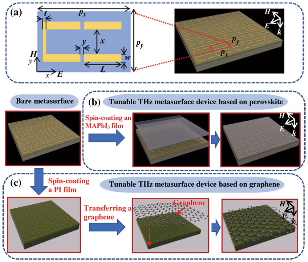
Fig. 1. Schematic of the fabrication process for the proposed (a) perovskite-based and (b) graphene-based controllable THz asymmetric metasurface devices. (c) Unit cell of the bare metasurface with parameters: p y = 190 μm p x = 255 μm L = 75 μm x = 110 μm y = 20 μm w = 15 μm t = 3 μm
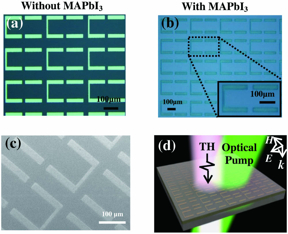
Fig. 2. Optical microscopy images of the bare metasurface device (a) without MAPbI 3 MAPbI 3
Fig. 3. Simulated transmission spectra, surface currents, and electric field distributions for (a) the perovskite-based symmetrical metasurface when the perovskite photoconductivity value is 0 S/m and the proposed perovskite-based THz metasurface device when the perovskite photoconductivity values are (b) 0 S/m and (c) 6000 S/m.
Fig. 4. (a) Simulated and (b) measured transmission spectra of the perovskite-based THz metasurface device for different values of perovskite photoconductivity and photoexcitation intensity. (c), (d) Variation of the transmission amplitude at frequencies f 1 f 2 f 3
Fig. 5. (a) Transmission spectra of analytical fits to the two-oscillator model for different values of perovskite photoconductivity. (b) Fit parameters as a function of the perovskite photoconductivity (κ THz 2
Fig. 6. (a) Three-dimensional schematic of the controllable graphene-based THz metasurface device with optical microscopy images on both sides. (b), (c) Diagrams of (b) optical modulation via pumping and (c) electrical modulation using bias voltages. (d) Raman spectra of the graphene layer measured with a 514 nm excitation laser at three different locations.
Fig. 7. (a) Transmission spectra of the simulation result from electromagnetic simulation software and analytical fitting curves by two-oscillator model under the different Fermi energy of graphene. Simulated electric field distributions at the frequency of transmission peak f 2 f 1 f 2 f 3 κ THz 2
Fig. 8. (a) Measured transmission spectra of the graphene-based THz metasurface device with varying Fermi energy and photoexcitation intensity. (b) Variation of the transmission amplitude at frequencies f 1 f 2 f 3
Fig. 9. (a) Measured transmission spectra of the graphene-based THz metasurface device with and without ion-gel film coating. (b) Electrical modulation of the transmission spectrum at different gate voltages.


Set citation alerts for the article
Please enter your email address

© Copyright 2018-2021 | Chinese Laser Press. All Rights Reserved 沪ICP备15018463号-20