Contents


2022
Volume: 10 Issue 10
23 Article(s)
Export citation format
NEXT-GENERATION SILICON PHOTONICS

Next-generation silicon photonics: introduction
Daoxin Dai, Di Liang, and Pavel Cheben
In the past decade, silicon photonics has been making tremendous progress in terms of device functionality and performances as well as circuit integration for many practical applications ranging from communication, sensing, and information processing. This special issue, including four review articles and nine research articles, aims to provide a comprehensive overview of this exciting field. They offer a collective summary of recent progresses, in-depth discussions of the state-of-the-art, and insights into forthcoming developments that are well poised to drive silicon photonics technology into its next generation.In the past decade, silicon photonics has been making tremendous progress in terms of device functionality and performances as well as circuit integration for many practical applications ranging from communication, sensing, and information processing. This special issue, including four review articles and nine research articles, aims to provide a comprehensive overview of this exciting field. They offer a collective summary of recent progresses, in-depth discussions of the state-of-the-art, and insights into forthcoming developments that are well poised to drive silicon photonics technology into its next generation..
Photonics Research
- Publication Date: Sep. 29, 2022
- Vol. 10, Issue 10, NGSP1 (2022)


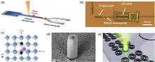
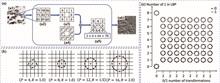
Silicon photonic devices for scalable quantum information applications | On the Cover
Lantian Feng, Ming Zhang, Jianwei Wang, Xiaoqi Zhou, Xiaogang Qiang, Guangcan Guo, and Xifeng Ren
With high integration density and excellent optical properties, silicon photonics is becoming a promising platform for complete integration and large-scale optical quantum information processing. Scalable quantum information applications need photon generation and detection to be integrated on the same chip, and we have seen that various devices on the silicon photonic chip have been developed for this goal. This paper reviews the relevant research results and state-of-the-art technologies on the silicon photonic chip for scalable quantum applications. Despite the shortcomings, the properties of some components have already met the requirements for further expansion. Furthermore, we point out the challenges ahead and future research directions for on-chip scalable quantum information applications.With high integration density and excellent optical properties, silicon photonics is becoming a promising platform for complete integration and large-scale optical quantum information processing. Scalable quantum information applications need photon generation and detection to be integrated on the same chip, and we have seen that various devices on the silicon photonic chip have been developed for this goal. This paper reviews the relevant research results and state-of-the-art technologies on the silicon photonic chip for scalable quantum applications. Despite the shortcomings, the properties of some components have already met the requirements for further expansion. Furthermore, we point out the challenges ahead and future research directions for on-chip scalable quantum information applications..
Photonics Research
- Publication Date: Sep. 14, 2022
- Vol. 10, Issue 10, A135 (2022)
OPTICAL METASURFACES: FUNDAMENTALS AND APPLICATIONS
Anisotropic Fermat’s principle for controlling hyperbolic van der Waals polaritons
Sicen Tao, Tao Hou, Yali Zeng, Guangwei Hu, Zixun Ge, Junke Liao, Shan Zhu, Tan Zhang, Cheng-Wei Qiu, and Huanyang Chen
Transformation optics (TO) facilitates flexible designs of spatial modulation of optical materials via coordinate transformations, thus, enabling on-demand manipulations of electromagnetic waves. However, the application of TO theory in control of hyperbolic waves remains elusive due to the spatial metric signature transition from (+,+) to (-,+) of a two-dimensional hyperbolic geometry. Here, we proposed a distinct Pythagorean theorem, which leads to establishing an anisotropic Fermat’s principle. It helps to construct anisotropic geometries and is a powerful tool for manipulating hyperbolic waves at the nanoscale and polaritons. Making use of absolute instruments, the excellent collimating and focusing behaviors of naturally in-plane hyperbolic polaritons in van der Waals α–MoO3 layers are demonstrated, which opens up a new way for polaritons manipulation.Transformation optics (TO) facilitates flexible designs of spatial modulation of optical materials via coordinate transformations, thus, enabling on-demand manipulations of electromagnetic waves. However, the application of TO theory in control of hyperbolic waves remains elusive due to the spatial metric signature transition from (
Photonics Research
- Publication Date: Sep. 30, 2022
- Vol. 10, Issue 10, B14 (2022)
Research Articles
Errata

Exciton binding energy and effective mass of CsPbCl3: a magneto-optical study: publisher’s note
Michal Baranowski, Paulina Plochocka, Rui Su, Laurent Legrand, Thierry Barisien, Frederick Bernardot, Qihua Xiong, Christophe Testelin, and Maria Chamarro
This publisher’s note corrects the author name spelling in Photon. Res.8, A50 (2020)10.1364/PRJ.401872.This publisher’s note corrects the author name spelling in Photon. Res. 8 , A50 (2020 )10.1364/PRJ.401872
Photonics Research
- Publication Date: Sep. 30, 2022
- Vol. 10, Issue 10, 2447 (2022)
Fiber Optics and Optical Communications
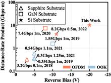
Si-substrate vertical-structure InGaN/GaN micro-LED-based photodetector for beyond 10 Gbps visible light communication | Spotlight on Optics
Jianyang Shi, Zengyi Xu, Wenqing Niu, Dong Li, Xiaoming Wu, Ziwei Li, Junwen Zhang, Chao Shen, Guangxu Wang, Xiaolan Wang, Jianli Zhang, Fengyi Jiang, Shaohua Yu, and Nan Chi
Visible light communication (VLC) has emerged as a promising communication method in 6G. However, the development of receiving devices is much slower than that of transmitting devices, limited by materials, structures, and fabrication. In this paper, we propose and fabricate an InGaN/GaN multiple-quantum-well-based vertical-structure micro-LED-based photodetector (μPD) on a Si substrate. A comprehensive comparison of the photoelectrical performance and communication performance of three sizes of μPDs, 10, 50, and 100 μm, is presented. The peak responsivity of all three μPDs is achieved at 400 nm, while the passband full-widths at half maxima are 87, 72, and 78 nm for 10, 50, and 100 μm μPDs, respectively. The -20 dB cutoff bandwidth is up to 822 MHz for 50 μm μPD. A data rate of 10.14 Gbps is experimentally demonstrated by bit and power loading discrete multitone modulation and the proposed digital pre-equalizer algorithm over 1 m free space utilizing the self-designed 4×4 50 μm μPD array as a receiver and a 450 nm laser diode as a transmitter. This is the first time a more than 10 Gbps VLC system has been achieved utilizing a GaN-based micro-PD, to the best of our knowledge. The investigation fully demonstrates the superiority of Si substrates and vertical structures in InGaN/GaN μPDs and shows its great potential for high-speed VLC links beyond 10 Gbps.Visible light communication (VLC) has emerged as a promising communication method in 6G. However, the development of receiving devices is much slower than that of transmitting devices, limited by materials, structures, and fabrication. In this paper, we propose and fabricate an InGaN/GaN multiple-quantum-well-based vertical-structure micro-LED-based photodetector (μPD) on a Si substrate. A comprehensive comparison of the photoelectrical performance and communication performance of three sizes of μPDs, 10, 50, and 100 μm, is presented. The peak responsivity of all three μPDs is achieved at 400 nm, while the passband full-widths at half maxima are 87, 72, and 78 nm for 10, 50, and 100 μm μPDs, respectively. The
Photonics Research
- Publication Date: Sep. 30, 2022
- Vol. 10, Issue 10, 2394 (2022)
Image Processing and Image Analysis
Speckle spatial correlations aiding optical transmission matrix retrieval: the smoothed Gerchberg–Saxton single-iteration algorithm
Daniele Ancora, Lorenzo Dominici, Antonio Gianfrate, Paolo Cazzato, Milena De Giorgi, Dario Ballarini, Daniele Sanvitto, and Luca Leuzzi
The estimation of the transmission matrix of a disordered medium is a challenging problem in disordered photonics. Usually, its reconstruction relies on a complex inversion that aims at connecting a fully controlled input to the deterministic interference of the light field scrambled by the device. At the moment, iterative phase retrieval protocols provide the fastest reconstructing frameworks, converging in a few tens of iterations. Exploiting the knowledge of speckle correlations, we construct a new phase retrieval algorithm that reduces the computational cost to a single iteration. Besides being faster, our method is practical because it accepts fewer measurements than state-of-the-art protocols. Thanks to reducing computation time by one order of magnitude, our result can be a step forward toward real-time optical imaging that exploits disordered devices.The estimation of the transmission matrix of a disordered medium is a challenging problem in disordered photonics. Usually, its reconstruction relies on a complex inversion that aims at connecting a fully controlled input to the deterministic interference of the light field scrambled by the device. At the moment, iterative phase retrieval protocols provide the fastest reconstructing frameworks, converging in a few tens of iterations. Exploiting the knowledge of speckle correlations, we construct a new phase retrieval algorithm that reduces the computational cost to a single iteration. Besides being faster, our method is practical because it accepts fewer measurements than state-of-the-art protocols. Thanks to reducing computation time by one order of magnitude, our result can be a step forward toward real-time optical imaging that exploits disordered devices..
Photonics Research
- Publication Date: Sep. 27, 2022
- Vol. 10, Issue 10, 2349 (2022)
Rapid full-color Fourier ptychographic microscopy via spatially filtered color transfer
Jiurun Chen, Aiye Wang, An Pan, Guoan Zheng, Caiwen Ma, and Baoli Yao
Full-color imaging is of critical importance in digital pathology for analyzing labeled tissue sections. In our previous cover story [Sci. China: Phys., Mech. Astron.64, 114211 (2021)SCPMCL1674-734810.1007/s11433-021-1730-x], a color transfer approach was implemented on Fourier ptychographic microscopy (FPM) for achieving high-throughput full-color whole slide imaging without mechanical scanning. The approach was able to reduce both acquisition and reconstruction time of FPM by three-fold with negligible trade-off on color accuracy. However, the method cannot properly stain samples with two or more dyes due to the lack of spatial constraints in the color transfer process. It also requires a high computation cost in histogram matching of individual patches. Here we report a modified full-color imaging algorithm for FPM, termed color-transfer filtering FPM (CFFPM). In CFFPM, we replace the original histogram matching process with a combination of block processing and trilateral spatial filtering. The former step reduces the search of the solution space for colorization, and the latter introduces spatial constraints that match the low-resolution measurement. We further adopt an iterative process to refine the results. We show that this method can perform accurate and fast color transfer for various specimens, including those with multiple stains. The statistical results of 26 samples show that the average root mean square error is only 1.26% higher than that of the red-green-blue sequential acquisition method. For some cases, CFFPM outperforms the sequential method because of the coherent artifacts introduced by dust particles. The reported CFFPM strategy provides a turnkey solution for digital pathology via computational optical imaging.Full-color imaging is of critical importance in digital pathology for analyzing labeled tissue sections. In our previous cover story [Sci. China: Phys., Mech. Astron. 64 , 114211 (2021 )SCPMCL 1674-7348 10.1007/s11433-021-1730-x
Photonics Research
- Publication Date: Sep. 30, 2022
- Vol. 10, Issue 10, 2410 (2022)
Instrumentation and Measurements
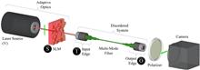
Particle manipulation behind a turbid medium based on the intensity transmission matrix
Kaige Liu, Hengkang Zhang, Shanshan Du, Zeqi Liu, Bin Zhang, Xing Fu, and Qiang Liu
Although optical tweezers can manipulate tiny particles, the distortion caused by the scattering medium restricts their application. Wavefront-shaping techniques such as the transmission matrix (TM) method are powerful tools to achieve light focusing behind the scattering medium. In this paper, we propose a method to focus light through a scattering medium in a large area based on the intensity transmission matrix (ITM). Only relying on the intensity distribution, we can calculate the ITM with the number of measurements equal to that of the control segments. Free of the diffraction limit, our method guarantees high energy usage of the light field. Based on this method, we have implemented particle manipulation with a high degree of freedom on single and multiple particles. In addition, the manipulation range is enlarged more than 20 times (compared to the memory effect) to 200 μm.Although optical tweezers can manipulate tiny particles, the distortion caused by the scattering medium restricts their application. Wavefront-shaping techniques such as the transmission matrix (TM) method are powerful tools to achieve light focusing behind the scattering medium. In this paper, we propose a method to focus light through a scattering medium in a large area based on the intensity transmission matrix (ITM). Only relying on the intensity distribution, we can calculate the ITM with the number of measurements equal to that of the control segments. Free of the diffraction limit, our method guarantees high energy usage of the light field. Based on this method, we have implemented particle manipulation with a high degree of freedom on single and multiple particles. In addition, the manipulation range is enlarged more than 20 times (compared to the memory effect) to 200 μm..
Photonics Research
- Publication Date: Sep. 14, 2022
- Vol. 10, Issue 10, 2293 (2022)
Integrated Optics

Ultra-high-linearity integrated lithium niobate electro-optic modulators | Editors' Pick
Hanke Feng, Ke Zhang, Wenzhao Sun, Yangming Ren, Yiwen Zhang, Wenfu Zhang, and Cheng Wang
Integrated lithium niobate (LN) photonics is a promising platform for future chip-scale microwave photonics systems owing to its unique electro-optic properties, low optical loss, and excellent scalability. A key enabler for such systems is a highly linear electro-optic modulator that could faithfully convert analog electrical signals into optical signals. In this work, we demonstrate a monolithic integrated LN modulator with an ultra-high spurious-free dynamic range (SFDR) of 120.04 dB·Hz4/5 at 1 GHz, using a ring-assisted Mach–Zehnder interferometer configuration. The excellent synergy between the intrinsically linear electro-optic response of LN and an optimized linearization strategy allows us to fully suppress the cubic terms of third-order intermodulation distortions (IMD3) without active feedback controls, leading to ∼20 dB improvement over previous results in the thin-film LN platform. Our ultra-high-linearity LN modulators could become a core building block for future large-scale functional microwave photonic integrated circuits by further integration with other high-performance components like low-loss delay lines, tunable filters, and phase shifters available on the LN platform.Integrated lithium niobate (LN) photonics is a promising platform for future chip-scale microwave photonics systems owing to its unique electro-optic properties, low optical loss, and excellent scalability. A key enabler for such systems is a highly linear electro-optic modulator that could faithfully convert analog electrical signals into optical signals. In this work, we demonstrate a monolithic integrated LN modulator with an ultra-high spurious-free dynamic range (SFDR) of
Photonics Research
- Publication Date: Sep. 27, 2022
- Vol. 10, Issue 10, 2366 (2022)
Gain-enabled optical delay readout unit using CMOS-compatible avalanche photodetectors
Ranjan Das, Yanran Xie, Henry Frankis, Keru Chen, Hermann Rufenacht, Guillaume Lamontagne, Jonathan D. B. Bradley, and Andrew P. Knights
A compact time delay unit is fundamental to integrated photonic circuits with applications in, for example, optical beam-forming networks, photonic equalization, and finite and infinite impulse response optical filtering. In this paper, we report a novel gain-enabled delay readout system using a tunable optical carrier, low-frequency RF signal and CMOS-compatible photodetectors, suitable for silicon photonic integration. The characterization method relies on direct phase measurement of an input RF signal and thereafter extraction of the delay profile. Both integrated silicon and germanium photodetectors coupled with low-bandwidth electronics are used to characterize a microring resonator-based, true-time delay unit under distinct ring–bus coupling formats. The detectors, used in both linear and avalanche mode, are shown to be successful as optical-to-electrical converters and RF amplifiers without introducing significant phase distortion. For a Si–Ge separate-absorption-charge-multiplication avalanche detector, an RF amplification of 10 dB is observed relative to a Ge PIN linear detector. An all-silicon defect-mediated avalanche photodetector is shown to have a 3 dB RF amplification compared to the same PIN detector. All ring delay measurement results are validated by full-wave simulation. Additionally, the impact of photodetector biasing and system linearity is analyzed.A compact time delay unit is fundamental to integrated photonic circuits with applications in, for example, optical beam-forming networks, photonic equalization, and finite and infinite impulse response optical filtering. In this paper, we report a novel gain-enabled delay readout system using a tunable optical carrier, low-frequency RF signal and CMOS-compatible photodetectors, suitable for silicon photonic integration. The characterization method relies on direct phase measurement of an input RF signal and thereafter extraction of the delay profile. Both integrated silicon and germanium photodetectors coupled with low-bandwidth electronics are used to characterize a microring resonator-based, true-time delay unit under distinct ring–bus coupling formats. The detectors, used in both linear and avalanche mode, are shown to be successful as optical-to-electrical converters and RF amplifiers without introducing significant phase distortion. For a Si–Ge separate-absorption-charge-multiplication avalanche detector, an RF amplification of 10 dB is observed relative to a Ge PIN linear detector. An all-silicon defect-mediated avalanche photodetector is shown to have a 3 dB RF amplification compared to the same PIN detector. All ring delay measurement results are validated by full-wave simulation. Additionally, the impact of photodetector biasing and system linearity is analyzed..
Photonics Research
- Publication Date: Sep. 30, 2022
- Vol. 10, Issue 10, 2422 (2022)
Lasers and Laser Optics
High-power wavelength-tunable and power-ratio-controllable dual-wavelength operation at 1319 nm and 1338 nm in a Q-switched Nd:YAG laser
Qi Bian, Yong Bo, Jun-Wei Zuo, Lei Yuan, Hong-Wei Gao, and Qin-Jun Peng
We report the first demonstration on three types of 1.3 μm spectral region in a Q-switched Nd:YAG laser. In order to dissipate the heat deposition effectively to obtain good beam quality, the Nd:YAG rod crystal with 1° cut-angle on end faces is side-pumped by the quasi-continuous-wave pulsed laser diode. A Suprasil etalon is well designed as the intracavity mode-selector to obtain wavelength-tunable single line or power-ratio-controllable dual line operation at 1319 nm and 1338 nm. With the pump pulse width of 200 μs and pump power of 410 W, the acousto-optic Q-switched laser delivered a pulse width of 117 ns at 400 Hz repetition rate, and the M2 factor was measured to be about 1.87. 1319 nm together with 1338 nm single-wavelength laser achieved an average output power of 47.6 W and 39.9 W with a linewidth of 0.48 nm and 0.32 nm, and a tunable range of 111.2 pm and 108.6 pm, respectively. Among dual-wavelength oscillation, both lines can be tuned at almost equal intensity level with 45.7 W total output power, which is input into an LBO crystal to generate red light of 11.4 W for 659 nm, 6.7 W for 664 nm, and 7.5 W for 669 nm. The 1.3 μm wavelength-selectable operation realized by using the same laser configuration may enhance the application in the fields of tunable lasers and THz frequency generation.We report the first demonstration on three types of 1.3 μm spectral region in a
Photonics Research
- Publication Date: Sep. 14, 2022
- Vol. 10, Issue 10, 2287 (2022)
Nonlinear Optics
Hybrid plasmonic–dielectric metal-nanowire coupler for high-efficiency broadband nonlinear frequency conversion
Kui-Ying Nie, Song Luo, Fang-Fang Ren, Xuanhu Chen, Shulin Gu, Zhanghai Chen, Rong Zhang, and Jiandong Ye
Pursuing nanometer-scale nonlinear converters based on second harmonic generation (SHG) is a stimulating strategy for bio-sensing, on-chip optical circuits, and quantum information processing, but the light-conversion efficiency is still poor in such ultra-small dimensional nanostructures. Herein, we demonstrate a highly enhanced broadband frequency converter through a hybrid plasmonic–dielectric coupler, a ZnTe/ZnO single core–shell nanowire (NW) integrated with silver (Ag) nanoparticles (NPs). The NW dimension has been optimized to allow the engineering of dielectric resonances at both fundamental wave and second harmonic frequencies. Meanwhile, the localized surface plasmon resonances are excited in the regime between the Ag NPs and ZnTe/ZnO dielectric NW, as evidenced by plasmon-enhanced Raman scattering and resonant absorption. These two contributors remarkably enhance local fields and consequently support the strong broadband SHG outputs in this hybrid nanostructure by releasing stringent phase-matching conditions. The proposed nanoscale nonlinear optical converter enables the manipulation of nonlinear light–matter interactions toward the development of on-chip nanophotonic systems.Pursuing nanometer-scale nonlinear converters based on second harmonic generation (SHG) is a stimulating strategy for bio-sensing, on-chip optical circuits, and quantum information processing, but the light-conversion efficiency is still poor in such ultra-small dimensional nanostructures. Herein, we demonstrate a highly enhanced broadband frequency converter through a hybrid plasmonic–dielectric coupler, a ZnTe/ZnO single core–shell nanowire (NW) integrated with silver (Ag) nanoparticles (NPs). The NW dimension has been optimized to allow the engineering of dielectric resonances at both fundamental wave and second harmonic frequencies. Meanwhile, the localized surface plasmon resonances are excited in the regime between the Ag NPs and ZnTe/ZnO dielectric NW, as evidenced by plasmon-enhanced Raman scattering and resonant absorption. These two contributors remarkably enhance local fields and consequently support the strong broadband SHG outputs in this hybrid nanostructure by releasing stringent phase-matching conditions. The proposed nanoscale nonlinear optical converter enables the manipulation of nonlinear light–matter interactions toward the development of on-chip nanophotonic systems..
Photonics Research
- Publication Date: Sep. 26, 2022
- Vol. 10, Issue 10, 2337 (2022)
Optical and Photonic Materials
Taming quantum dots’ nucleation and growth enables stable and efficient blue-light-emitting devices
Zhiwei Ma, Junxia Hu, Liping Tang, and Bingbing Lyu
Controlling quantum dots’ emission, nanostructure, and energy level alignment to achieve stable and efficient blue emission is of great significance for electroluminescence devices but remains a challenge. Here, a series of blue ZnCdSeS/ZnS quantum dots was optimized in preparation by taming their nucleation and growth kinetics. Controlling anion precursor reactive properties to modulate quantum dots’ nucleation and growth tailors their alloy core and continuous gradient energy band nanostructure. These results not only elevate the thermal stability of blue quantum dots but also further enhance the injection/transportation of carriers and improve the radiative recombination efficiency in the device. The blue ZnCdSeS/ZnS quantum dots applied in light-emitting devices show superior performance, including maximum current efficiency and external quantum efficiency of, respectively, 8.2 cd/A and 15.8% for blue, 2.6 cd/A and 10.0% for blue-violet, and 10.9 cd/A and 13.4% for sky-blue devices. The blue and sky-blue devices exhibit lifetimes of more than 10,000 h. The proposed methodology for tailoring quantum dots is expected to pave new guidelines for further facilitating visible optoelectronic device exploration.Controlling quantum dots’ emission, nanostructure, and energy level alignment to achieve stable and efficient blue emission is of great significance for electroluminescence devices but remains a challenge. Here, a series of blue ZnCdSeS/ZnS quantum dots was optimized in preparation by taming their nucleation and growth kinetics. Controlling anion precursor reactive properties to modulate quantum dots’ nucleation and growth tailors their alloy core and continuous gradient energy band nanostructure. These results not only elevate the thermal stability of blue quantum dots but also further enhance the injection/transportation of carriers and improve the radiative recombination efficiency in the device. The blue ZnCdSeS/ZnS quantum dots applied in light-emitting devices show superior performance, including maximum current efficiency and external quantum efficiency of, respectively, 8.2 cd/A and 15.8% for blue, 2.6 cd/A and 10.0% for blue-violet, and 10.9 cd/A and 13.4% for sky-blue devices. The blue and sky-blue devices exhibit lifetimes of more than 10,000 h. The proposed methodology for tailoring quantum dots is expected to pave new guidelines for further facilitating visible optoelectronic device exploration..
Photonics Research
- Publication Date: Sep. 27, 2022
- Vol. 10, Issue 10, 2359 (2022)
Optical Devices
Compact nano-void spectrometer based on a stable engineered scattering system
Qi Sun, Przemyslaw Falak, Tom Vettenburg, Timothy Lee, David B. Phillips, Gilberto Brambilla, and Martynas Beresna
Random scattering of light in disordered media can be used for highly sensitive speckle-based wavemeters and spectrometers. However, the multiple scattering events that fold long optical paths within a compact space also make such devices exceedingly sensitive to vibrations and small disturbances to the disordered media. Here, we show how scattering can be engineered so that it can be used for a compact computational spectrometer that is largely insensitive to environmental factors. We designed and fabricated a three-dimensional pseudo-random nano-void pattern with 62% scattering efficiency. The controlled amount of multiple scattering ensured a sufficiently long optical path for the target resolution of 100 pm, with optimal long-term stability. The 200-μm-thick scattering silica substrate was integrated in a compact assembly with a low-cost camera sensor. The target resolution was achieved for full spectrum measurements while single wavelengths could be determined with 50 pm resolution. Such tailored scattering systems can improve the trade-off among cost, size, stability, and spectral resolution in computational spectrometers.Random scattering of light in disordered media can be used for highly sensitive speckle-based wavemeters and spectrometers. However, the multiple scattering events that fold long optical paths within a compact space also make such devices exceedingly sensitive to vibrations and small disturbances to the disordered media. Here, we show how scattering can be engineered so that it can be used for a compact computational spectrometer that is largely insensitive to environmental factors. We designed and fabricated a three-dimensional pseudo-random nano-void pattern with 62% scattering efficiency. The controlled amount of multiple scattering ensured a sufficiently long optical path for the target resolution of 100 pm, with optimal long-term stability. The 200-μm-thick scattering silica substrate was integrated in a compact assembly with a low-cost camera sensor. The target resolution was achieved for full spectrum measurements while single wavelengths could be determined with 50 pm resolution. Such tailored scattering systems can improve the trade-off among cost, size, stability, and spectral resolution in computational spectrometers..
Photonics Research
- Publication Date: Sep. 26, 2022
- Vol. 10, Issue 10, 2328 (2022)
High-precision whispering gallery microsensors with ergodic spectra empowered by machine learning
Bing Duan, Hanying Zou, Jin-Hui Chen, Chun Hui Ma, Xingyun Zhao, Xiaolong Zheng, Chuan Wang, Liang Liu, and Daquan Yang
Whispering gallery mode (WGM) microcavities provide increasing opportunities for precision measurement due to their ultrahigh sensitivity, compact size, and fast response. However, the conventional WGM sensors rely on monitoring the changes of a single mode, and the abundant sensing information in WGM transmission spectra has not been fully utilized. Here, empowered by machine learning (ML), we propose and demonstrate an ergodic spectra sensing method in an optofluidic microcavity for high-precision pressure measurement. The developed ML method realizes the analysis of the full features of optical spectra. The prediction accuracy of 99.97% is obtained with the average error as low as 0.32 kPa in the pressure range of 100 kPa via the training and testing stages. We further achieve the real-time readout of arbitrary unknown pressure within the range of measurement, and a prediction accuracy of 99.51% is obtained. Moreover, we demonstrate that the ergodic spectra sensing accuracy is ∼11.5% higher than that of simply extracting resonating modes’ wavelength. With the high sensitivity and prediction accuracy, this work opens up a new avenue for integrated intelligent optical sensing.Whispering gallery mode (WGM) microcavities provide increasing opportunities for precision measurement due to their ultrahigh sensitivity, compact size, and fast response. However, the conventional WGM sensors rely on monitoring the changes of a single mode, and the abundant sensing information in WGM transmission spectra has not been fully utilized. Here, empowered by machine learning (ML), we propose and demonstrate an ergodic spectra sensing method in an optofluidic microcavity for high-precision pressure measurement. The developed ML method realizes the analysis of the full features of optical spectra. The prediction accuracy of 99.97% is obtained with the average error as low as 0.32 kPa in the pressure range of 100 kPa via the training and testing stages. We further achieve the real-time readout of arbitrary unknown pressure within the range of measurement, and a prediction accuracy of 99.51% is obtained. Moreover, we demonstrate that the ergodic spectra sensing accuracy is
Photonics Research
- Publication Date: Sep. 26, 2022
- Vol. 10, Issue 10, 2343 (2022)
Optoelectronics
High-frequency enhanced response based on Sb2Te3 topological insulators
Shi Zhang, Chaofan Shi, Weiwei Tang, Libo Zhang, Li Han, Chengsen Yang, Zhengyang Zhang, Jian Wang, Miao Cai, Guanhai Li, Changlong Liu, Lin Wang, Xiaoshuang Chen, and Wei Lu
Topological insulators represent a new quantum phase of matter with spin-polarized surface states that are protected from backscattering, exhibiting electronic responses to light, such as topological quantum phase transitions. However, the effects of high-frequency driving topological intrinsic systems have remained largely unexplored challenges experimentally for high-sensitivity terahertz detection. In this study, by integrating Sb2Te3 topological insulators with subwavelength metal antennas through micro-nano processing, a high-frequency terahertz detector with high sensitivity is proposed. The enhanced response originates from the asymmetric scattering of the surface electrons in the Sb2Te3 flakes induced by the terahertz wave. The device displays room-temperature photodetection with a responsivity of 192 mA/W and equivalent noise power of less than 0.35 nW/Hz1/2 in the frequency range from 0.02 to 0.3 THz. These results pave the way for the exploitation of topological insulators for high-frequency operation in real-time imaging within long-wavelength optoelectronics.Topological insulators represent a new quantum phase of matter with spin-polarized surface states that are protected from backscattering, exhibiting electronic responses to light, such as topological quantum phase transitions. However, the effects of high-frequency driving topological intrinsic systems have remained largely unexplored challenges experimentally for high-sensitivity terahertz detection. In this study, by integrating
Photonics Research
- Publication Date: Sep. 14, 2022
- Vol. 10, Issue 10, 2302 (2022)
Systematic investigation of millimeter-wave optic modulation performance in thin-film lithium niobate
Yiwen Zhang, Linbo Shao, Jingwei Yang, Zhaoxi Chen, Ke Zhang, Kam-Man Shum, Di Zhu, Chi Hou Chan, Marko Lončar, and Cheng Wang
Millimeter-wave (mmWave) band (30–300 GHz) is an emerging spectrum range for wireless communication, short-range radar, and sensor applications. mmWave-optic modulators that could efficiently convert mmWave signals into the optical domain are crucial components for long-haul transmission of mmWave signals through optical networks. At these ultrahigh frequencies, however, the modulation performances are highly sensitive to the transmission line loss as well as the velocity- and impedance-matching conditions, while precise measurements and modeling of these parameters are often non-trivial. Here we present a systematic investigation of the mmWave-optic modulation performances of thin-film lithium niobate modulators through theoretical modeling, electrical verifications, and electro-optic measurements at frequencies up to 325 GHz. Based on our experimentally verified model, we demonstrate thin-film lithium niobate mmWave-optic modulators with a measured 3-dB electro-optic bandwidth of 170 GHz and a 6-dB bandwidth of 295 GHz. The device also shows a low RF half-wave voltage of 7.3 V measured at an ultrahigh modulation frequency of 250 GHz. This work provides a comprehensive guideline for the design and characterization of mmWave-optic modulators and paves the way toward future integrated mmWave photonic systems for beyond-5G communication and radar applications.Millimeter-wave (mmWave) band (30–300 GHz) is an emerging spectrum range for wireless communication, short-range radar, and sensor applications. mmWave-optic modulators that could efficiently convert mmWave signals into the optical domain are crucial components for long-haul transmission of mmWave signals through optical networks. At these ultrahigh frequencies, however, the modulation performances are highly sensitive to the transmission line loss as well as the velocity- and impedance-matching conditions, while precise measurements and modeling of these parameters are often non-trivial. Here we present a systematic investigation of the mmWave-optic modulation performances of thin-film lithium niobate modulators through theoretical modeling, electrical verifications, and electro-optic measurements at frequencies up to 325 GHz. Based on our experimentally verified model, we demonstrate thin-film lithium niobate mmWave-optic modulators with a measured 3-dB electro-optic bandwidth of 170 GHz and a 6-dB bandwidth of 295 GHz. The device also shows a low RF half-wave voltage of 7.3 V measured at an ultrahigh modulation frequency of 250 GHz. This work provides a comprehensive guideline for the design and characterization of mmWave-optic modulators and paves the way toward future integrated mmWave photonic systems for beyond-5G communication and radar applications..
Photonics Research
- Publication Date: Sep. 28, 2022
- Vol. 10, Issue 10, 2380 (2022)
Ultrahigh frame rate digital light projector using chip-scale LED-on-CMOS technology
Navid Bani Hassan, Fahimeh Dehkhoda, Enyuan Xie, Johannes Herrnsdorf, Michael J. Strain, Robert Henderson, and Martin D. Dawson
Digital light projector systems are crucial components in applications, including computational imaging, fluorescence microscopy, and highly parallel data communications. Current technology based on digital micromirror displays are limited to absolute frame rates in the few tens of kiloframes per second and require the use of external light sources and coupling optics. Furthermore, to realize gray-scale pixel values using duty cycle control, frame rates are reduced proportionally to the number of gray levels required. Here we present a self-emissive chip-scale projector system based on micro-LED pixels directly bonded to a smart pixel CMOS drive chip. The 128×128 pixel array can project binary patterns at up to 0.5 Mfps and toggle between two stored frames at megahertz rates. The projector has a 5-bit gray-scale resolution that can be updated at up to 83 kfps, and can be held in memory as a constant bias for the binary pattern projection. Additionally, the projector can be operated in a pulsed mode, with individual pixels emitting pulses down to a few nanoseconds in duration. Again, this mode can be used in conjunction with the high-speed spatial pattern projection. As a demonstration of the data throughput achievable with this system, we present an optical camera communications application, exhibiting data rates of >5 Gb/s.Digital light projector systems are crucial components in applications, including computational imaging, fluorescence microscopy, and highly parallel data communications. Current technology based on digital micromirror displays are limited to absolute frame rates in the few tens of kiloframes per second and require the use of external light sources and coupling optics. Furthermore, to realize gray-scale pixel values using duty cycle control, frame rates are reduced proportionally to the number of gray levels required. Here we present a self-emissive chip-scale projector system based on micro-LED pixels directly bonded to a smart pixel CMOS drive chip. The
Photonics Research
- Publication Date: Sep. 30, 2022
- Vol. 10, Issue 10, 2434 (2022)
Physical Optics
Phase regimes of parity-time-symmetric coupled-ring systems at exceptional points
Zhuang Ma, Xiaoyan Zhou, and Lin Zhang
The optical coupled resonant system consisting of an integrated resonator with gain and a resonator with loss provides an excellent platform to create exceptional points (EPs) in non-Hermitian systems. Most previous studies have focused on the striking intensity feature of EPs, but its phase response is seldom investigated. In this work, we present a thorough study on the phase response of an EP system. Intriguingly, the phase response exhibits distinct behavior depending on the ordering of the ring resonators: when the input light in a bus waveguide is coupled directly or indirectly to the ring with a gain, the phase response is featured by nonmonotonic transition and 2π monotonic transition, respectively. We also prove that the newly identified phase features are theoretically guaranteed. These phase responses produce unique group delays that have never been found in other coupled resonant systems. The results deepen our understanding on EPs in non-Hermitian systems and are potentially useful for practical applications exploiting phase features.The optical coupled resonant system consisting of an integrated resonator with gain and a resonator with loss provides an excellent platform to create exceptional points (EPs) in non-Hermitian systems. Most previous studies have focused on the striking intensity feature of EPs, but its phase response is seldom investigated. In this work, we present a thorough study on the phase response of an EP system. Intriguingly, the phase response exhibits distinct behavior depending on the ordering of the ring resonators: when the input light in a bus waveguide is coupled directly or indirectly to the ring with a gain, the phase response is featured by nonmonotonic transition and
Photonics Research
- Publication Date: Sep. 28, 2022
- Vol. 10, Issue 10, 2374 (2022)
Quantum Optics
Hong–Ou–Mandel interference linking independent room-temperature quantum memories | Editors' Pick
Chao-Ni Zhang, Hang Li, Jian-Peng Dou, Feng Lu, Hong-Zhe Yang, Xiao-Ling Pang, and Xian-Min Jin
To realize a large-scale quantum network, both quantum memory and the interference of retrieved indistinguishable photons are essentially required to perform multi-photon synchronization and quantum-interference-mediated entanglement swapping. Significant progress has been achieved in low-temperature and well-isolated systems. However, linking independent quantum memories at room temperature remain challenging. Here, we present an experimental demonstration of Hong–Ou–Mandel interference between single photons from two independent room-temperature quantum memories. We manage to simultaneously operate two such quantum memories and individually obtain a memory-built-in quantum correlation of Stokes and anti-Stokes photons by a far-off-resonance Duan–Lukin–Cirac–Zoller protocol. We also successfully enhance the Hong–Ou–Mandel interference rate up to about 15 times by increasing each photon rate, which is achieved by coordinating two quantum memories with a repeat-until-success fashion. We observe the visibility of quantum interference up to 75.0% without reduction of any background noise, well exceeding the classical limit of 50%. Our results, together with its straightforward, broadband, and room-temperature features, open up a promising way towards realizing large-scale quantum networks at ambient conditions.To realize a large-scale quantum network, both quantum memory and the interference of retrieved indistinguishable photons are essentially required to perform multi-photon synchronization and quantum-interference-mediated entanglement swapping. Significant progress has been achieved in low-temperature and well-isolated systems. However, linking independent quantum memories at room temperature remain challenging. Here, we present an experimental demonstration of Hong–Ou–Mandel interference between single photons from two independent room-temperature quantum memories. We manage to simultaneously operate two such quantum memories and individually obtain a memory-built-in quantum correlation of Stokes and anti-Stokes photons by a far-off-resonance Duan–Lukin–Cirac–Zoller protocol. We also successfully enhance the Hong–Ou–Mandel interference rate up to about 15 times by increasing each photon rate, which is achieved by coordinating two quantum memories with a repeat-until-success fashion. We observe the visibility of quantum interference up to 75.0% without reduction of any background noise, well exceeding the classical limit of 50%. Our results, together with its straightforward, broadband, and room-temperature features, open up a promising way towards realizing large-scale quantum networks at ambient conditions..
Photonics Research
- Publication Date: Sep. 29, 2022
- Vol. 10, Issue 10, 2388 (2022)
Surface Optics and Plasmonics
Flexible manipulation of plasmon dephasing time via the adjustable Fano asymmetric dimer
Yang Xu, Yulu Qin, Peng Lang, Boyu Ji, Xiaowei Song, and Jingquan Lin
It is highly desirable to flexibly and actively manipulate the dephasing time of a plasmon in many potential applications; however, this remains a challenge. In this work, by using femtosecond time-resolved photoemission electron microscopy, we experimentally demonstrated that the Fano resonance mode in the asymmetric nanorod dimer can greatly extend the dephasing time of a femtosecond plasmon, whereas the non-Fano resonance results in a smaller dephasing time due to the large radiative damping, and flexible manipulation of the dephasing time can be realized by adjusting one of the nanorods in the Fano asymmetric dimer. Interestingly, it was found that plasmon resonance wavelengths both appeared red-shifted as the length of the upper or lower nanorods increased individually, but the dephasing time varied. Furthermore, it also indicated that the dephasing time can be prolonged with a smaller ascending rate by increasing the length of both the nanorods simultaneously while keeping the dimer asymmetry. Meanwhile, the roles of radiative and nonradiative damping in dephasing time are unveiled in the process of nanorod length variation. These results are well supported by numerical simulations and calculations.It is highly desirable to flexibly and actively manipulate the dephasing time of a plasmon in many potential applications; however, this remains a challenge. In this work, by using femtosecond time-resolved photoemission electron microscopy, we experimentally demonstrated that the Fano resonance mode in the asymmetric nanorod dimer can greatly extend the dephasing time of a femtosecond plasmon, whereas the non-Fano resonance results in a smaller dephasing time due to the large radiative damping, and flexible manipulation of the dephasing time can be realized by adjusting one of the nanorods in the Fano asymmetric dimer. Interestingly, it was found that plasmon resonance wavelengths both appeared red-shifted as the length of the upper or lower nanorods increased individually, but the dephasing time varied. Furthermore, it also indicated that the dephasing time can be prolonged with a smaller ascending rate by increasing the length of both the nanorods simultaneously while keeping the dimer asymmetry. Meanwhile, the roles of radiative and nonradiative damping in dephasing time are unveiled in the process of nanorod length variation. These results are well supported by numerical simulations and calculations..
Photonics Research
- Publication Date: Sep. 14, 2022
- Vol. 10, Issue 10, 2267 (2022)
High-sensitivity modulation of electromagnetically induced transparency analog in a THz asymmetric metasurface integrating perovskite and graphene
Tongling Wang, Tengteng Li, Haiyun Yao, Yuying Lu, Xin Yan, Maoyong Cao, Lanju Liang, Maosheng Yang, and Jianquan Yao
Active control of the electromagnetically induced transparency (EIT) analog is desirable in photonics development. Here, we theoretically and experimentally proposed a novel terahertz (THz) asymmetric metasurface structure that can possess high-sensitivity modulation under extremely low power density by integrating perovskite or graphene. Using the novel metasurface structure with the perovskite coating, the maximum amplitude modulation depth (AMD) of this perovskite-based device reached 490.53% at a low power density of 12.8037 mW/cm2. In addition, after the novel THz metasurface structure was combined with graphene, this graphene-based device also achieved high AMD with the maximum AMD being 180.56% at 16.312 mW/cm2, and its transmission amplitude could be electrically driven at a low bias voltage. The physical origin of this modulation was explained using a two-oscillator EIT model. This work provides a promising platform for developing high-sensitivity THz sensors, light modulators, and switches.Active control of the electromagnetically induced transparency (EIT) analog is desirable in photonics development. Here, we theoretically and experimentally proposed a novel terahertz (THz) asymmetric metasurface structure that can possess high-sensitivity modulation under extremely low power density by integrating perovskite or graphene. Using the novel metasurface structure with the perovskite coating, the maximum amplitude modulation depth (AMD) of this perovskite-based device reached 490.53% at a low power density of
Photonics Research
- Publication Date: Sep. 26, 2022
- Vol. 10, Issue 10, 2317 (2022)
Ultrafast Optics
High-quality 8-fold self-compression of ultrashort near-UV pulses in an Ar-filled ultrathin-walled photonic crystal fiber
Jie Luan, Philip St.J. Russell, and David Novoa
We demonstrate generation of 7.6 fs near-UV pulses centered at 400 nm via 8-fold soliton-effect self-compression in an Ar-filled hollow-core kagomé-style photonic crystal fiber with ultrathin core walls. Analytical calculations of the effective compression length and soliton order permit adjustment of the experimental parameters, and numerical modeling of the nonlinear pulse dynamics in the fiber accurately predicts the spectrotemporal profiles of the self-compressed pulses. After compensation of phase distortion introduced by the optical elements along the beam path from the fiber to the diagnostics, 71% of the pulse energy was in the main temporal lobe, with peak powers in excess of 0.2 GW. The convenient setup opens up new opportunities for time-resolved studies in spectroscopy, chemistry, and materials science.We demonstrate generation of 7.6 fs near-UV pulses centered at 400 nm via 8-fold soliton-effect self-compression in an Ar-filled hollow-core kagomé-style photonic crystal fiber with ultrathin core walls. Analytical calculations of the effective compression length and soliton order permit adjustment of the experimental parameters, and numerical modeling of the nonlinear pulse dynamics in the fiber accurately predicts the spectrotemporal profiles of the self-compressed pulses. After compensation of phase distortion introduced by the optical elements along the beam path from the fiber to the diagnostics, 71% of the pulse energy was in the main temporal lobe, with peak powers in excess of 0.2 GW. The convenient setup opens up new opportunities for time-resolved studies in spectroscopy, chemistry, and materials science..
Photonics Research
- Publication Date: Sep. 30, 2022
- Vol. 10, Issue 10, 2405 (2022)
Errata
Exciton binding energy and effective mass of CsPbCl3: a magneto-optical study: publisher’s note
Michal Baranowski, Paulina Plochocka, Rui Su, Laurent Legrand, Thierry Barisien, Frederick Bernardot, Qihua Xiong, Christophe Testelin, and Maria Chamarro
This publisher’s note corrects the author name spelling in Photon. Res.8, A50 (2020)10.1364/PRJ.401872.This publisher’s note corrects the author name spelling in Photon. Res. 8 , A50 (2020 )10.1364/PRJ.401872
Photonics Research
- Publication Date: Sep. 30, 2022
- Vol. 10, Issue 10, 2447 (2022)

About the Cover
Photonic integrated circuit is the most attractive way to enhance the complexity of quantum optical experiments. Here we give a review about the relevant research results and state-of-the-art technologies on the silicon photonic chips for scalable quantum applications.
© Copyright 2018-2021 | Chinese Laser Press. All Rights Reserved 沪ICP备15018463号-20