1School of Information and Automation Engineering, Qilu University of Technology (Shandong Academy of Sciences), Jinan 250353, China
2State Key Laboratory of Dynamic Measurement Technology, North University of China, Taiyuan 030051, China
3School of Opto-electronic Engineering, Zaozhuang University, Zaozhuang 277160, China
4Precision Optical Manufacturing and Testing Centre, Shanghai Institute of Optics and Fine Mechanics, Chinese Academy of Sciences, Shanghai 201800, China
5School of Electrical and Optoelectronic Engineering, West Anhui University, Lu’an 237000, China
Active control of the electromagnetically induced transparency (EIT) analog is desirable in photonics development. Here, we theoretically and experimentally proposed a novel terahertz (THz) asymmetric metasurface structure that can possess high-sensitivity modulation under extremely low power density by integrating perovskite or graphene. Using the novel metasurface structure with the perovskite coating, the maximum amplitude modulation depth (AMD) of this perovskite-based device reached 490.53% at a low power density of . In addition, after the novel THz metasurface structure was combined with graphene, this graphene-based device also achieved high AMD with the maximum AMD being 180.56% at , and its transmission amplitude could be electrically driven at a low bias voltage. The physical origin of this modulation was explained using a two-oscillator EIT model. This work provides a promising platform for developing high-sensitivity THz sensors, light modulators, and switches.
1. INTRODUCTION
Metasurfaces, also known as two-dimensional (2D) metamaterials, possess extraordinary electromagnetic properties unavailable in nature, which have opened up a new way to manipulate electromagnetic propagation [1–3]. Among them, electromagnetically induced transparency (EIT) attempting to induce it in 2D metasurfaces mimics the quantum interference effect, breaking the rigorous conditions for its implementation in three-level atomic systems [4–6]. The analog of EIT in metasurfaces generally occurs as a result of destructive interference and shows significant potential for applications in sensing [7], slow light devices [8], and enhancing nonlinear interactions [9]. Following the Federal Communications Commission’s decision to open the terahertz (THz) frequency range from 95 GHz to 3 THz for sixth generation (6G) experiments in 2019 [10], metasurface-based devices that realize the EIT effect at THz frequencies have received further attention [11–14]. In particular, active control of EIT in metasurface THz devices is highly desirable.
Recently, many kinds of research have focused on the modulation of the EIT effect at THz frequencies by integrating metasurfaces with dynamic materials [15–19]. Among them, perovskite and graphene have emerged as promising platforms for tunable THz metasurface devices that benefit from their unique electromagnetic and optical properties. Methylammonium lead iodine ( or ), in a class of metal halide perovskites, exhibits significant power conversion efficiencies, reaching 20% [20]. Perovskites also have other advantageous properties [21–23]; in particular, their free carrier density can be tuned dynamically under optical stimulation, making an excellent choice for tunable metasurface THz devices [24,25]. Furthermore, it can be prepared as a thin film through a solution process, which greatly simplifies the fabrication of perovskite-based metasurface devices [26]. In addition, graphene, a 2D, single-layer carbon lattice, possesses remarkable electronic, mechanical, and thermal properties, including fast carrier mobility and tunability [27]. The tunability of the surface conductivity of graphene makes it another good candidate for modulating THz waves in metasurfaces [28].
Accordingly, combinations of perovskite and graphene have stimulated research interest for EIT modulation in THz metasurface devices. Manjappa et al. realized dynamic control of Fano resonance, an EIT-like effect, by integrating perovskite with a metasurface THz device. The degree of photoexcitation of perovskite acted as a photoswitch to adjust the strength of the resonant coupling [29]. Kim et al. experimentally investigated an electrically tunable analog of EIT in a graphene-based metasurface THz device. The transparency peak could be modulated by applying different voltages, with a maximum amplitude modulation depth (AMD) of 25% [30]. Liu et al. presented a numerical and theoretical study of an EIT metasurface device based on a simple graphene resonator, which realized the manipulation of the EIT effect at THz frequencies [31]. Li et al. designed, fabricated, and measured a graphene-silicon integrated metasurface THz device whose Fano resonance was modulated by changing the conductivity of graphene with optical and electrical stimuli [32]. Extensive related work has focused on numerical simulations, and some suffer from insufficient modulation effects, so the realization of high-sensitivity, controllable EIT-like metasurface devices at THz frequencies has also remained an experimental challenge.
Sign up for Photonics Research TOC. Get the latest issue of Photonics Research delivered right to you!Sign up now
In this paper, we propose a novel asymmetric metasurface structure that possesses high-sensitivity modulation performance and experimentally demonstrate optical and electrical modulation of the Fano-type EIT effect at THz frequencies by integrating the proposed asymmetric metasurface with either perovskite or graphene. Increased laser power density caused a reduction in the amplitude of the transparency window of perovskite-based and graphene-based devices in both experiments and simulations. The maximum AMDs of the perovskite- and graphene-based devices reached 490.53% and 180.56% under extremely low power densities of and , respectively. Moreover, the transmission amplitude of the graphene-based device could be electrically driven at a low bias voltage. We also employed the two-oscillator EIT model to theoretically describe the modulation of the EIT-like effect in the metasurface devices, and the results agreed well with the simulation results. Our work could offer promising steps toward realization of tunable metasurface devices in the THz, infrared, and optical regions.
2. MATERIALS AND METHODS
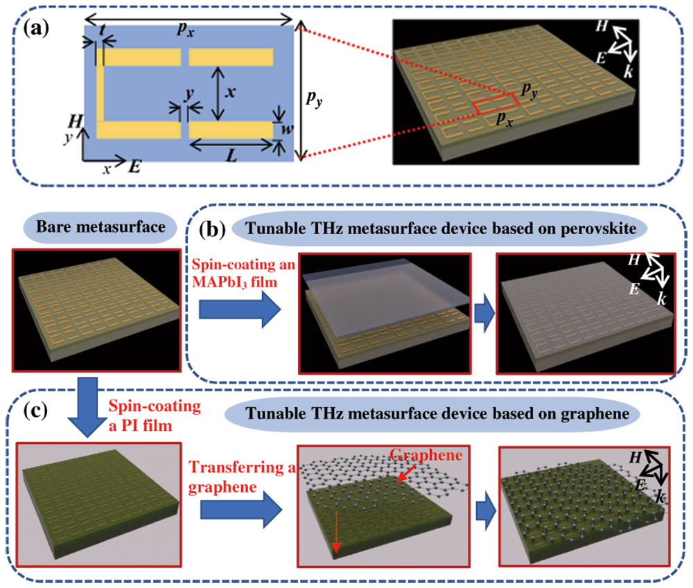
Figure 1 illustrates the fabrication of the proposed THz asymmetric metasurface based on either perovskite or graphene. The bare metasurface devices were fabricated in a two-step process. First, a polyimide (PI) film of thickness 10 μm was coated over a 500-μm-thick quartz glass substrate. The permittivity of the PI was 3.1 with a loss tangent of 0.05. Next, an array of 200-nm-thick asymmetrical gold structures was deposited on the PI film using conventional photolithography. The conductivity of the gold was . The geometrical parameters of the gold structures, defined in Fig. 1(a), are μ, μ, μ, μ, and μ. The periodicities, and , of the unit cell are 190 μm and 255 μm, respectively. Arrays of asymmetrical gold unit cells serve as the building blocks of the device, which can exhibit the EIT-like effect at THz frequencies as Fano-type linear destructive interference [33].
Figure 1.Schematic of the fabrication process for the proposed (a) perovskite-based and (b) graphene-based controllable THz asymmetric metasurface devices. (c) Unit cell of the bare metasurface with parameters: μ, μ, μ, μ, μ, μ, and μ.
A schematic of the asymmetric metasurface device based on perovskite is shown in Fig. 1(b) with an film spin-coated on the bare metasurface device. Figure 1(c) shows a graphical representation of fabricating the graphene-based device. A , three-layer graphene sheet was transferred onto the device after the bare surface was spin-coated with a PI film. The graphene layer was grown using the copper-catalyzed chemical vapor deposition method.
In experiments, a terahertz time-domain spectroscopy (THz-TDS) system was used to optically characterize the devices. The incident THz source illuminates the device along the axis, with the polarization of the electric field along the axis.
To clarify the mechanism of the proposed devices, numerical simulations were performed utilizing the Computer Simulation Technology (CST) Microwave Studio based on the finite integral techniques. “Periodic” boundary conditions with Floquet-port were applied along the and axes, and the “open (add space)” boundary condition was applied along the axis. Plane wave is incident along the unit cell of the proposed device from the port on the surface side with the electric field along the axis as the excitation source, while the transmission spectra were obtained from the port placed on the other side of the device. The photoconductivity of the perovskite in simulation was varied to simulate the effect of pump power density in the experiment [34]. The surface conductivity of graphene can be characterized by the Drude model. In the frequency domain (), it can be expressed as
denotes the Fermi energy, is the reduced Planck’s constant, and is the electronic charge. The relaxation rate, , can be given by , where is the electron mobility, and is the Fermi velocity. The relative complex permittivity can be written as , where is the thickness of the graphene.
3. RESULTS AND DISCUSSION
A. High-Sensitivity Modulation of EIT in a Perovskite-Based THz Metasurface Device
The perovskite-based THz metasurface device architecture is shown in Fig. 2. Top-view optical microscopy images of the metasurface without and with the perovskite coating are shown in Figs. 2(a) and 2(b), respectively. Figure 2(b) shows that the film was spin-coated onto the metasurface device with good uniformity. The representative top-view scanning electron microscopy image of the proposed perovskite-based device is exhibited in Fig. 2(c). Figure 2(d) shows a schematic of the perovskite-based THz metasurface device illuminated by a THz beam and 2-mm-diameter green laser. In experiments, a THz-TDS system with the polarization of incident THz radiation parallel to the bar of the gold structures was used to characterize the device after optical pumping with a 532 nm laser. The interaction between the normally incident THz wave and the device generates EIT. The laser excites the free carriers and excitons of perovskite, and varying the laser power achieves modulation of the device’s transmission.
Figure 2.Optical microscopy images of the bare metasurface device (a) without film and (b) with spin-coated . (c) Representative top-view scanning electron microscopy image of the proposed perovskite-based device. (d) Graphical representation of the proposed perovskite-based THz metasurface device illuminated by a THz beam and optical pump.
Figure 3(a) shows the simulated transmission spectra for the perovskite-based symmetrical metasurface when the perovskite photoconductivity value is 0 S/m. Under the incident electric polarization along the axis, the symmetrical structure exhibits only single broad resonance at the frequency of 1.02 THz. We simulated the surface currents and electric field distributions at the resonance frequency to understand the nature of resonances in the symmetric structure. It can be seen that there are symmetric parallel currents along the direction of the electric polarization and only a bright dipolar resonance can be excited, which results in a broad dipole resonance. Once the symmetry is broken, simulated transmission spectra of the proposed perovskite-based THz metasurface device at perovskite photoconductivity values of 0 S/m and 6000 S/m are shown in Figs. 3(b) and 3(c). It can be concluded from Fig. 3(a) that the EIT effect is caused by conductive coupling within the unit cell of the metasurface structure. The vertical metal strip connecting the upper and lower horizontal bars of the gold structure breaks its symmetry, which excites the electric quadrupole mode, and a transparency window can be observed at 0.9 THz between two resonance dips. To better understand the mechanism of the EIT effect, we simulated the surface current and electric field distributions at the frequency of the transmission peak, 0.9 THz. Quadrupolar resonance with the out-of-phase oscillation can be excited by introducing the structural asymmetry leading to a destructive interference. As a result of the destructive interference, radiative loss of the THz beam can be suppressed, and a transparency window appears in the transmission spectrum, realizing the Fano-type EIT effect. The transmission of the perovskite-based device can be modulated by optically tuning the film’s photoconductivity. When the photoconductivity of the perovskite is increased to 6000 S/m [Fig. 3(b)], the amplitude of the transparency window is strongly reduced because more free carriers are generated in the perovskite film. Correspondingly, the intensity of the electric field distribution exhibits a remarkable decrease.
Figure 3.Simulated transmission spectra, surface currents, and electric field distributions for (a) the perovskite-based symmetrical metasurface when the perovskite photoconductivity value is 0 S/m and the proposed perovskite-based THz metasurface device when the perovskite photoconductivity values are (b) 0 S/m and (c) 6000 S/m.
Figure 4 shows both simulated and measured modulation of EIT in the perovskite-based THz metasurface device. In the absence of an external optical pump—that is, when the perovskite photoconductivity is zero—we observe a strong Fano-type EIT effect because of destructive interference in the unit cell of the asymmetric structure, shown by the black solid curves in Figs. 4(a) and 4(b). However, because the photoconductivity of the film is optically tunable, optical pumping can be used to tune the EIT transmission amplitude. When the photoconductivity of the perovskite increases under optical pumping [blue, gray, and red curves in Figs. 4(a) and 4(b)], the amplitude of the transparency window is reduced in both the simulated and experimental results. The change in simulated or measured transmittance at the frequencies marked is shown in Figs. 4(c) and 4(d). In the simulation [Fig. 4(c)], increasing the perovskite photoconductivity caused the transmission amplitude at (black stars) to increase from 0.1543 to 0.43034, and the amplitude at (green squares) to increase from 0.1764 to 0.447, while the transmission amplitude at (blue circles) gradually decreased from 0.928 to 0.578. The experiments are fundamentally identical to the results from simulations, which means the amplitude of the transmission can be modulated to some extent by changing the laser power density. As shown in Fig. 4(d), increasing the density in the experiment caused the amplitudes at and to increase from 0.095 to 0.225 and from 0.095 to 0.561, respectively, while the amplitude at decreased from 0.75 to 0.538.
Figure 4.(a) Simulated and (b) measured transmission spectra of the perovskite-based THz metasurface device for different values of perovskite photoconductivity and photoexcitation intensity. (c), (d) Variation of the transmission amplitude at frequencies , , and when changing (c) the photoconductivity of perovskite in the simulation or (d) the laser power density in the experiment. (e), (f) Amplitude modulation depth calculated by (e) simulation and (f) experiment.
We defined the AMD as , where , and and are the transmission amplitudes of the device with and without photoexcitation. Figures 4(e) and 4(f) show the AMD as a function of incident THz wave frequency and either the photoconductivity of perovskite [in the simulation, Fig. 4(e)] or the laser power density [in the experiment, Fig. 4(f)]. In Fig. 4(f), the AMD reaches up to 136.84% at or 490.53% at when the laser power density is only , which means that the transmission amplitude of the perovskite-based device can be modulated at extremely low laser power densities. For the frequency of transmission peak , the modulation depth was 38.3% and 28.3% in the simulation and experiment. The origin of the transmission amplitude modulation is the optically tunable photoconductivity of the film. Although the modulation depth is not high at the transmission peak, the perovskite-based THz metasurface device at the frequency of transmission dip can offer a very sensitive photoactive transmission switch under low power densities of continuous wave excitation, as low as .
Next, we employed the two-oscillator EIT model [35] to quantitatively describe the modulation of the EIT effect in our devices. The interference inside the asymmetrical metasurface structures can be described by the two-oscillator EIT model as [36,37] where and , and , and and refer to the resonance amplitudes, frequencies, and damping factors of the bright and dark modes. After solving Eqs. (2) and (3) with the approximation , the susceptibility of the asymmetry metasurface can be expressed as [12,38,39]where is proportional to the energy loss. The transmission of the device is . We used this expression to fit the simulated transmission spectra at different values of the perovskite photoconductivity, with , , and as parameters. Figure 5(a) reveals good agreement between the simulated [Fig. 4(a)] and fitted spectra, which confirms the validity of the simulated and observed Fano-type EIT modulation. Figure 5(b) shows the values of the fit parameters as a function of photoconductivity, which can reveal the damping mechanism. The coupling coefficient (black stars) is nearly inversely proportional to the perovskite photoconductivity. In other words, the parameter experiences a gradually decrease, which indicates the coupling strength of destructive interference between the bright and dark modes weakening with increasing photoconductivity. It is found that the damping factors (blue circles) and (green squares) gradually increase as the photoconductivity of perovskite increases, which means that the losses in the bright and dark modes enhance hampering the destructive interference. Among them, the variation of is higher than attributed to the damping rate of the bright mode dominated in the modulation process. Therefore, the increasing damping rates indicate that the value of the perovskite photoconductivity affects the local field at the asymmetrical metasurface, leading to the damping of the EIT effect at high conductivities. Such quantitative results further confirm that the perovskite photoconductivity increasing with photoexcitation can reduce the strength of transparency window.
Figure 5.(a) Transmission spectra of analytical fits to the two-oscillator model for different values of perovskite photoconductivity. (b) Fit parameters as a function of the perovskite photoconductivity ( is in units of ).
B. High-Sensitivity Modulation of EIT in a Graphene-Based THz Metasurface Device
Next, we fabricated the graphene-based THz metasurface device by transferring a , three-layer graphene sheet onto the same bare metasurface with asymmetrical gold structures used in the previous section. Figure 6(a) shows the device architecture and three optical microscopy images at three different locations, illustrating that the graphene was transferred onto the surface with good uniformity. Modulation of the EIT effect in the graphene-based device is achieved by changing the graphene’s Fermi energy through optical pumping or application of an external bias voltage, thus controlling the conductivity of the graphene. Figure 6(b) shows a graphical representation of optical modulation via a 532 nm continuous wave laser with a 2 mm spot size. To realize electrical control, a solid-state ion-gel film was coated onto the graphene, and two electrodes composed of conductive ionic liquid were solidified onto the graphene layer and the ion-gel film, as illustrated in Fig. 6(c). In addition, Raman spectra of the three-layer graphene sheet were recorded at three different locations to further confirm the graphene’s quality. Under a 514 nm excitation laser, the D peaks () almost vanish, and the 2D peaks () with full width at half-maximum are much shorter than the G peaks (), implying that the graphene was of high quality.
Figure 6.(a) Three-dimensional schematic of the controllable graphene-based THz metasurface device with optical microscopy images on both sides. (b), (c) Diagrams of (b) optical modulation via pumping and (c) electrical modulation using bias voltages. (d) Raman spectra of the graphene layer measured with a 514 nm excitation laser at three different locations.
For the proposed graphene-based device, the transmission spectra of the simulation result from electromagnetic simulation software and analytical fitting curves by the two-oscillator model under the different Fermi energies of graphene are shown in Fig. 7(a). It can be concluded from Fig. 7(a) that the amplitude of the simulated transmission peak gradually decreases with increasing Fermi energy, while the transmission of the two valleys increases. This shows that the transmission of the graphene-based device can be modulated by changing the Fermi energy of the graphene. In addition, we used the two-oscillator EIT model to explain the physical origin of the controllable Fano-type EIT effect in the graphene-based device. Using Eqs. (2)–(4) in Section 3.A, we analytically fit the simulated transmission spectra with different Fermi energies, as shown in the right side of Fig. 7(a), which exhibit good agreement with the simulated results. Besides, Fig. 8(e) shows the fitting parameters , , and at different Fermi energies. The variation of the three parameters is almost consistent with the theoretical results for the perovskite-based device in Fig. 5(b). During modulation, the coupling coefficient is inversely proportional to the Fermi energy, which indicates weakened coupling in the metasurface as the Fermi energy increases from 0.01 eV to 0.1 eV. The damping factors and , regarded as the decay rates, increase with increasing Fermi energy. Hence, the strength of the transparency window is reduced by increasing the Fermi energy, achieving modulation of the transmission amplitude.
Figure 7.(a) Transmission spectra of the simulation result from electromagnetic simulation software and analytical fitting curves by two-oscillator model under the different Fermi energy of graphene. Simulated electric field distributions at the frequency of transmission peak when the Fermi energy are (b) 0.01 eV and (c) 0.1 eV. (d) Variation of the transmission amplitude at the frequency of , , and when changing the Fermi energy of graphene in simulation. (e) Fitting parameters as a function of the Fermi energy (the unit of is ).
Figure 8.(a) Measured transmission spectra of the graphene-based THz metasurface device with varying Fermi energy and photoexcitation intensity. (b) Variation of the transmission amplitude at frequencies , , and when changing the laser power density in the experiment. (c) Modulation depth amplitude calculated by experiment.
To further understand the physical behavior of the Fano-type EIT effect in the graphene-based device, the surface electric field distributions of the metasurface were simulated at the frequency of transmission peak , as shown in Figs. 7(b) and 7(c). It can be seen from Fig. 7(b) that the structural symmetry breaking enables the excitation of quadrupole mode with out-of-phase oscillation causing destructive interference, which can give rise to the Fano-type EIT effect. When the Fermi energy increases to 0.1 eV [Fig. 7(c)], the electric field strength is significantly reduced, resulting in a weakening of the transparency window. Figure 7(d) displays the relationship between the transmission amplitudes at the three frequencies indicated in Fig. 7(a) and the Fermi energy, which clearly indicates the modulation behavior of the transmission amplitude. Increasing the Fermi energy caused the transmission amplitude at (black stars) to increase from 0.129 to 0.493, and the amplitude at (green squares) to increase from 0.1205 to 0.511, while the transmission amplitude at the frequency of transmission peak (blue circles) gradually decreased from 0.869 to 0.59. Therefore, active control of the transmission amplitude can be realized by taking advantage of the tunable conductivity of graphene.
The transmission spectra of the graphene-based device were characterized using the THz-TDS scheme as shown in Fig. 8(a). In the experimental measurement, optical modulation of the transmission spectrum was implemented through 532 nm optical pumping, which excites more carriers in the graphene. Figure 8(a) shows the transmission spectra at different optical pump power densities, which are almost in accordance with the results of the simulation in Fig. 7(a). Without external optical stimulus, the transmission spectrum exhibits strong EIT with a transmission peak centered at between two transmission valleys. The transmission amplitude undergoes a significant change at very low power densities, . From Fig. 8(b), between 0 and , the transmission amplitudes of the valleys at frequencies and increase from 0.135 to 0.235 and 0.18 to 0.505, respectively, while the transmission peak at decreases from 0.732 to 0.52. These experimental results indicate that the EIT of the graphene-based device can be dynamically modulated through optical pumping that controls the conductivity of graphene. Figure 7(c) shows the AMD of the graphene-based device as a function of frequency. Upon increasing the laser power density in the experiment, the AMD increases in the two transmission valleys, although it increases only slightly at in the experiment. The maximum AMD at is 180.56% under a low power density of . Thus, the high-sensitivity transmission amplitude modulation in the graphene-based device can be achieved by changing the Fermi energy of graphene with external power densities as low as of continuous wave laser illumination.
Figure 9 shows the transmission spectra of the graphene-based device under electrical control, which indicates that modulation of the transmission amplitude can also be realized electrically. Because the dielectric loss of the ion-gel film damps the resonance coupling in the metasurface, the EIT undergoes a significant reduction and a slight redshift compared with the surface without the ion-gel film, as illustrated in Fig. 9(a). A variable bias voltage (0–0.8 V) was applied across the two solidified electrodes, and the resulting transmission spectra are shown in Fig. 9(b). It can be seen that the EIT effect can also be modulated by applying low voltages, but we do not analyze the effect further because the modulation ranges are small compared with the effect of optical modulation.
Figure 9.(a) Measured transmission spectra of the graphene-based THz metasurface device with and without ion-gel film coating. (b) Electrical modulation of the transmission spectrum at different gate voltages.
We demonstrated the high-sensitivity modulation of the EIT-like effect in a novel THz asymmetric metasurface by integrating perovskite or graphene. The perovskite- and graphene-based devices both exhibited a large modulation range in their transmission spectra under very low continuous wave power densities. The experimental results showed that the maximum AMD of the perovskite- and graphene-based devices reached 490.53% and 180.56% at and , respectively, in good agreement with simulations. Moreover, theoretical analysis based on the two-oscillator EIT model explained the physical origin of the controllable EIT-like effect, which further validated the modulation behavior of the transmission amplitude. The observed high-sensitivity modulation of the EIT analog in these devices has potential applications to THz sensors, light modulators, THz communications, and THz switching devices.
APPENDIX A: DEVICE FABRICATION
Perovskite-Based THz Metasurface Device
To fabricate the bare metasurface device, a 500-μm-thick quartz glass substrate was coated with a PI film of thickness 10 μm, and an array of asymmetrical gold structures 200-nm-thick was patterned onto the film with a mask using a conventional photolithography technique. Next, the perovskite precursor solution was prepared by dissolving 1.3 mol/L and 0.3 mol/L (MAI) in a solvent of N,N-dimethylformamide and dimethyl sulfoxide at a volume ratio of 9:1. The precursor solution was spin-coated onto the metasurface at 6000 r/min for 15 s, followed by spin-coating of an MAI/isopropyl alcohol solution at 4500 r/min for 45 s. Finally, the device was pre-annealed at 70°C for 20 s and annealed at 100°C for 30 min.
Graphene-Based THz Metasurface Device
An approximately 2-μm-thick PI film was spin-coated onto a bare metasurface device. Next, a , three-layer graphene sheet was directly attached to the PI film using the wet transfer method. To allow electrical modulation, a solid-state ion-gel film was coated onto graphene, and two electrodes composed of conductive ionic liquid were solidified onto the graphene layer and the ion-gel film.