• Photonics Research
  • Vol. 10, Issue 1, 261 (2022)
Shaonan Zheng, Hong Cai, Linfang Xu, Nanxi Li*, Zhonghua Gu, Yao Zhang, Weiguo Chen, Yanyan Zhou, Qingxin Zhang, and Lennon Yao Ting Lee
Author Affiliations
  • Institute of Microelectronics, A*STAR (Agency for Science, Technology and Research), Singapore 138634, Singapore
  • show less
    DOI: 10.1364/PRJ.439434 Cite this Article Set citation alerts
    Shaonan Zheng, Hong Cai, Linfang Xu, Nanxi Li, Zhonghua Gu, Yao Zhang, Weiguo Chen, Yanyan Zhou, Qingxin Zhang, Lennon Yao Ting Lee. Silicon substrate-integrated hollow waveguide for miniaturized optical gas sensing[J]. Photonics Research, 2022, 10(1): 261 Copy Citation Text show less
    (a) Schematic of a spiral iHWG etched on a silicon wafer substrate. (b) Cross section of the spiral iHWG. (c) Schematic assembly of LED, Si-iHWG, and PD. Drawings in (a)–(c) are not to scale. (d) Ray trajectory simulation in the spiral Si-iHWG. The source rays are the rays at 15° (angle between light ray and the x axis) and an axial ray in the x direction from a point emitter.
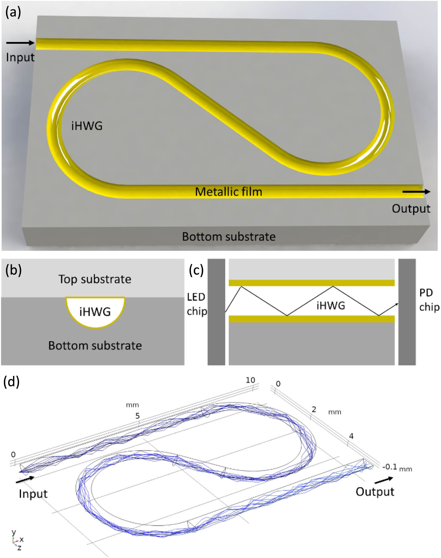
    Fig. 1. (a) Schematic of a spiral iHWG etched on a silicon wafer substrate. (b) Cross section of the spiral iHWG. (c) Schematic assembly of LED, Si-iHWG, and PD. Drawings in (a)–(c) are not to scale. (d) Ray trajectory simulation in the spiral Si-iHWG. The source rays are the rays at 15° (angle between light ray and the x axis) and an axial ray in the x direction from a point emitter.
    Fabrication process of Si-iHWG with a semicircular cross section. Drawing is not to scale. Two silicon wafers are used, one as the bottom wafer for Si-iHWG formation and the other as the top covering wafer to form the top part of the Si-iHWG. The top wafer and the bottom wafer are bonded together to form the Si-iHWG.
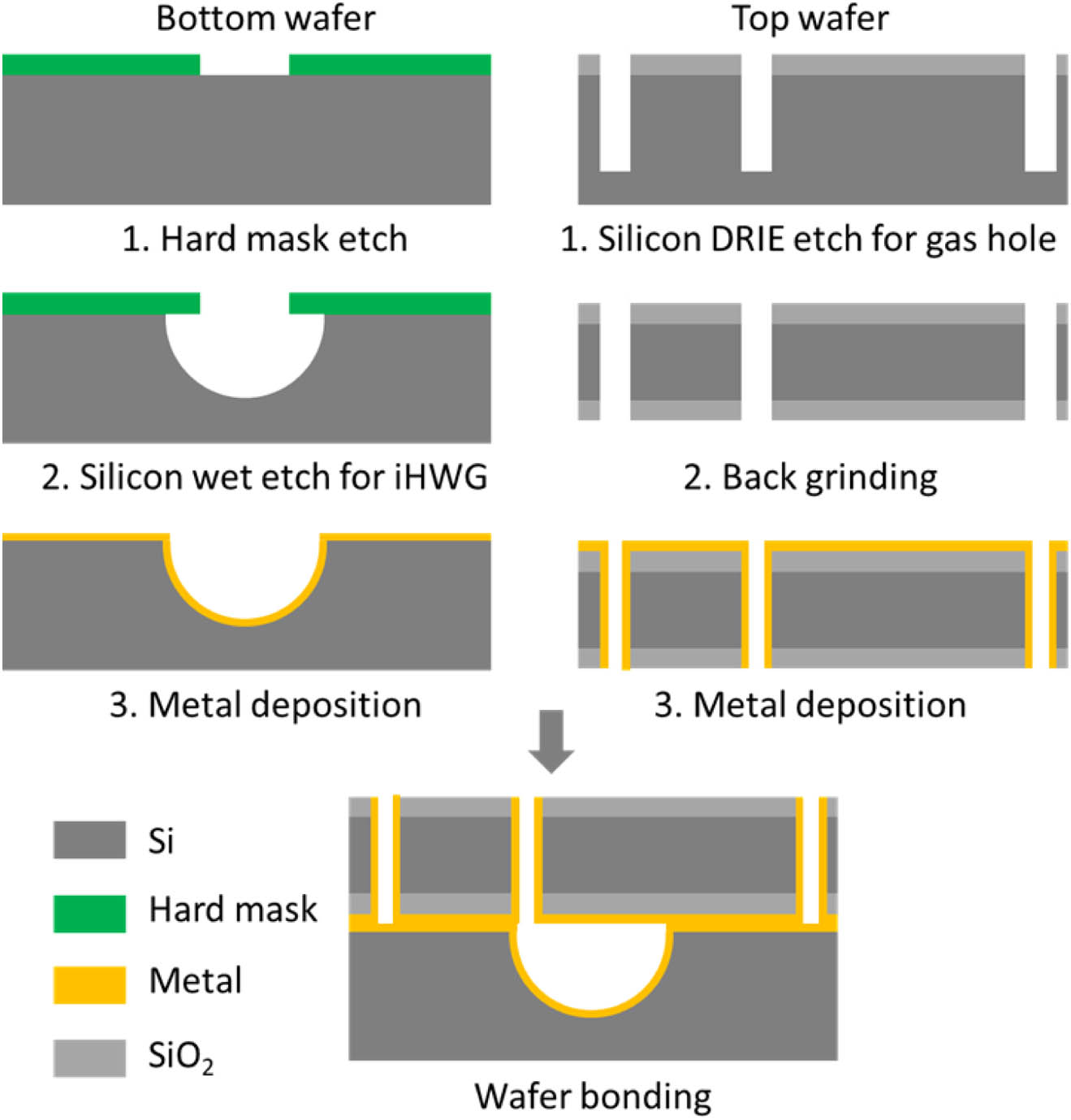
    Fig. 2. Fabrication process of Si-iHWG with a semicircular cross section. Drawing is not to scale. Two silicon wafers are used, one as the bottom wafer for Si-iHWG formation and the other as the top covering wafer to form the top part of the Si-iHWG. The top wafer and the bottom wafer are bonded together to form the Si-iHWG.
    (a) Optical micrograph of a Si-iHWG chip consisting of a straight Si-iHWG and a spiral Si-iHWG. The chip footprint is 10 mm×9 mm. (b) SEM image of the Si-iHWG cross section after silicon wet etching on the bottom wafer substrate. (c) SEM image of a spiral Si-iHWG after silicon wet etching on the bottom wafer substrate. (d) SEM image of the Si-iHWG cross section after wafer bonding.
    Fig. 3. (a) Optical micrograph of a Si-iHWG chip consisting of a straight Si-iHWG and a spiral Si-iHWG. The chip footprint is 10mm×9  mm. (b) SEM image of the Si-iHWG cross section after silicon wet etching on the bottom wafer substrate. (c) SEM image of a spiral Si-iHWG after silicon wet etching on the bottom wafer substrate. (d) SEM image of the Si-iHWG cross section after wafer bonding.
    Experimental setup for Si-iHWG loss characterization. ZBLAN: ZrF4-BaF2-LaF3-AlF3-NaF. A sample chip is placed at a six-axis optical fiber alignment system for loss characterization. A laptop is used for laser control and data acquisition from the detector.
    Fig. 4. Experimental setup for Si-iHWG loss characterization. ZBLAN: ZrF4-BaF2-LaF3-AlF3-NaF. A sample chip is placed at a six-axis optical fiber alignment system for loss characterization. A laptop is used for laser control and data acquisition from the detector.
    (a) Fully functional NDIR CO2 sensor prototype by assembling a Si-iHWG chip with off-chip LED and PD. (b) Side view of the Si-iHWG chip fixed by the holder.
    Fig. 5. (a) Fully functional NDIR CO2 sensor prototype by assembling a Si-iHWG chip with off-chip LED and PD. (b) Side view of the Si-iHWG chip fixed by the holder.
    Gas testing setup. Gas flows from two cylinders are precisely and independently controlled by two mass flow controllers (MFCs). The gas flow rate into sensor inlet is fixed at 500 standard cubic centimeters per minute (SCCM).
    Fig. 6. Gas testing setup. Gas flows from two cylinders are precisely and independently controlled by two mass flow controllers (MFCs). The gas flow rate into sensor inlet is fixed at 500 standard cubic centimeters per minute (SCCM).
    (a) Propagation loss of straight Si-iHWG. (b) Coupling loss between optical fiber and straight Si-iHWG. The error bars in (a) and (b) denote standard deviations of propagation loss from repeated measurements and coupling loss measured from the waveguides with five different lengths, respectively.
    Fig. 7. (a) Propagation loss of straight Si-iHWG. (b) Coupling loss between optical fiber and straight Si-iHWG. The error bars in (a) and (b) denote standard deviations of propagation loss from repeated measurements and coupling loss measured from the waveguides with five different lengths, respectively.
    (a) Output voltage from PD_s and PD_ref while changing CO2 concentration of mixed gas. The CO2 concentration is changed from 1000 ppm to 200 ppm at a concentration step of 50 ppm. N2 purging is performed every time before changing the CO2 concentration. (b) Relation between transmittance T and CO2 concentration. The data points are obtained by normalizing average value of Us with CO2 presence to baseline signal, i.e., average value of Us0 with N2 purging in each cycle.
    Fig. 8. (a) Output voltage from PD_s and PD_ref while changing CO2 concentration of mixed gas. The CO2 concentration is changed from 1000 ppm to 200 ppm at a concentration step of 50 ppm. N2 purging is performed every time before changing the CO2 concentration. (b) Relation between transmittance T and CO2 concentration. The data points are obtained by normalizing average value of Us with CO2 presence to baseline signal, i.e., average value of Us0 with N2 purging in each cycle.
    (a) Sensor response t while changing CO2 concentration of mixed gas. (b) Relation between sensor response t and CO2 concentration. The data points are the average values of sensor response t in each cycle. The error bars denote the standard deviations of sensor response t in each cycle.
    Fig. 9. (a) Sensor response t while changing CO2 concentration of mixed gas. (b) Relation between sensor response t and CO2 concentration. The data points are the average values of sensor response t in each cycle. The error bars denote the standard deviations of sensor response t in each cycle.
    Shaonan Zheng, Hong Cai, Linfang Xu, Nanxi Li, Zhonghua Gu, Yao Zhang, Weiguo Chen, Yanyan Zhou, Qingxin Zhang, Lennon Yao Ting Lee. Silicon substrate-integrated hollow waveguide for miniaturized optical gas sensing[J]. Photonics Research, 2022, 10(1): 261
    Download Citation