
Guohui Li, Rui Gao, Yue Han, Aiping Zhai, Yucheng Liu, Yue Tian, Bining Tian, Yuying Hao, Shengzhong Liu, Yucheng Wu, Yanxia Cui, "High detectivity photodetectors based on perovskite nanowires with suppressed surface defects," Photonics Res. 8, 1862 (2020)
- Photonics Research
- Vol. 8, Issue 12, 1862 (2020)
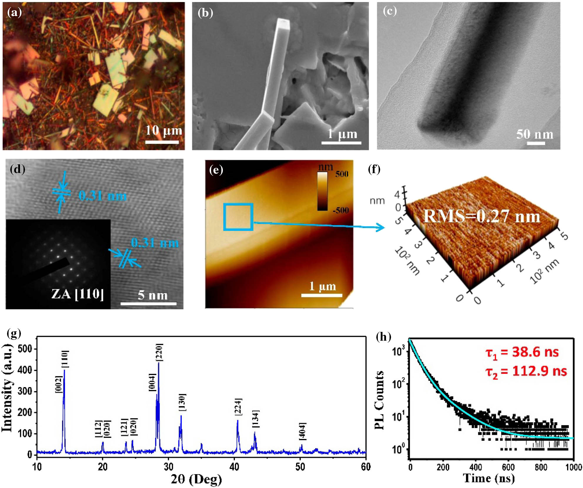
Fig. 1. (a) Optical image of MAPbI 3 PbAc 2 MAPbI 3 MAPbI 3 MAPbI 3 MAPbI 3 MAPbI 3 MAPbI 3 MAPbI 3
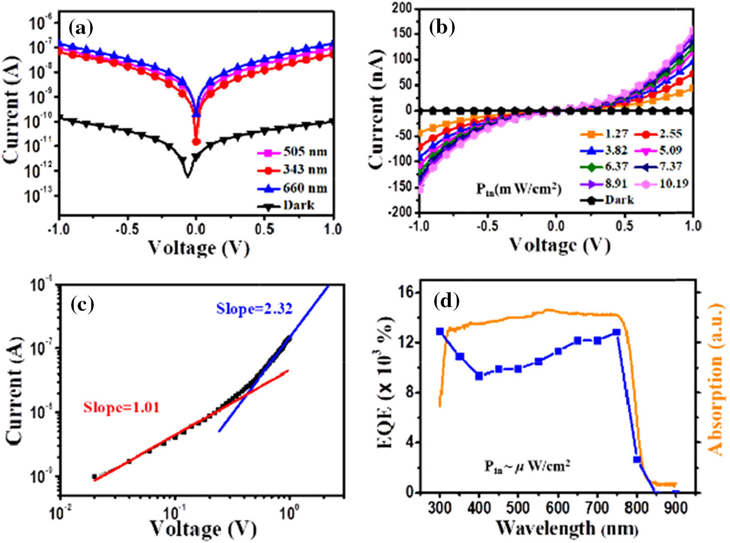
Fig. 2. (a) Logarithmic I - V 10.19 mW / cm 2 I - V I - V 10.19 mW / cm 2 MAPbI 3
Fig. 3. (a) Current versus illumination power density (i.e., LDR measurement) of the prepared photodetector under 532-nm continuous laser illumination. (b) External quantum efficiency (EQE) versus illumination power density. (c) Responsivity (R D *
Fig. 4. (a) Transient photo response measurement of the fabricated MAPbI 3 10.19 mW / cm 2 MAPbI 3
Fig. 5. Schematic illustration of the surface-initiated solution-growth strategy for preparing the single-crystalline MAPbI 3 PbAc 2 PbAc 2
Fig. 6. (a)–(d) Optical images of MAPbI 3 PbAc 2 MAPbI 3 MAPbI 3
Fig. 7. Experimental XRD pattern of as-grown MAPbI 3 MAPbI 3 MAPbI 3
Fig. 8. (a) Experimental XRD pattern of the MAPbI 3 MAPbI 3
Fig. 9. Microscopic characterizations of the as-grown MAPbI 3 MAPbI 3 MAPbI 3
Fig. 10. AFM morphology of the PEDOT:PSS surface. It has an average RMS value of 0.16 nm, only a bit lower than that of the as-grown MAPbI 3
Fig. 11. (a) Schematic diagram of the fabricated MSM-type MAPbI 3 MAPbI 3 ∼ 90 μm 2
Fig. 12. Dark and photo I - V MAPbI 3
Fig. 13. Measured dark-current noise at various frequencies for the MAPbI 3
Fig. 14. (a), (b) Illumination spectrum with power densities of ∼ μW / cm 2 MAPbI 3 I - V ∼ μW / cm 2 29.8 μW / cm 2 2 (d).
|
Table 1. Device Performance Comparison of Different Perovskite Nanowire Photodetectors Measured at Room Temperaturea


Set citation alerts for the article
Please enter your email address

© Copyright 2018-2021 | Chinese Laser Press. All Rights Reserved 沪ICP备15018463号-20