• Photonics Research
  • Vol. 8, Issue 12, 1862 (2020)
Guohui Li1、†, Rui Gao1、†, Yue Han1, Aiping Zhai1, Yucheng Liu2, Yue Tian1, Bining Tian1, Yuying Hao1, Shengzhong Liu2、3、4、5, Yucheng Wu1、6, and Yanxia Cui1、*
Author Affiliations
  • 1College of Physics and Optoelectronics, Key Laboratory of Advanced Transducers and Intelligent Control System of Ministry of Education, Key Laboratory of Interface Science and Engineering in Advanced Materials of Ministry of Education, Taiyuan University of Technology, Taiyuan 030024, China
  • 2Key Laboratory of Applied Surface and Colloid Chemistry, MOE; Shaanxi Key Laboratory for Advanced Energy Devices; Shaanxi Engineering Laboratory for Advanced Energy Technology, School of Materials Science and Engineering, Shaanxi Normal University, Xi’an 710119, China
  • 3Dalian National Laboratory for Clean Energy; iChEM, Dalian Institute of Chemical Physics, Chinese Academy of Sciences, Dalian 116023, China
  • 4University of Chinese Academy of Sciences, Beijing 100049, China
  • 5e-mail: liusz@snnu.edu.cn
  • 6e-mail: wyc@tyut.edu.cn
  • show less
    DOI: 10.1364/PRJ.403030 Cite this Article Set citation alerts
    Guohui Li, Rui Gao, Yue Han, Aiping Zhai, Yucheng Liu, Yue Tian, Bining Tian, Yuying Hao, Shengzhong Liu, Yucheng Wu, Yanxia Cui. High detectivity photodetectors based on perovskite nanowires with suppressed surface defects[J]. Photonics Research, 2020, 8(12): 1862 Copy Citation Text show less

    Abstract

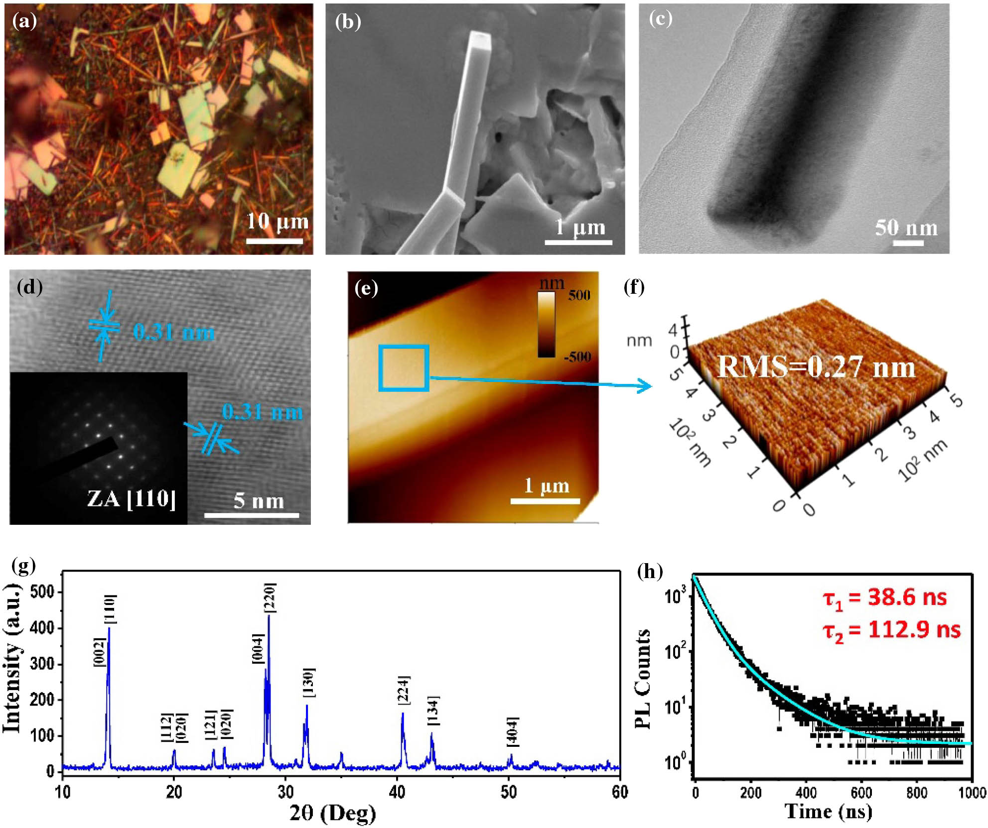
    Solution-processable, single-crystalline perovskite nanowires are ideal candidates for developing low-cost photodetectors, but their detectivities are limited due to a high level of unintentional defects. Through the surface-initiated solution-growth method, we fabricated high-quality, single-crystalline, defects-suppressed MAPbI3 nanowires, which possess atomically smooth side surfaces with a surface roughness of 0.27 nm, corresponding to a carrier lifetime of 112.9 ns. By forming ohmic MAPbI3/Au contacts through the dry contact method, high-performance metal–semiconductor–metal photodetectors have been demonstrated with a record large linear dynamic range of 157 dB along with a record high detectivity of 1.2×10¹⁴ Jones at an illumination power density of 5.5 nW/cm2. Such superior photodetector performance metrics are attributed to, first, the defects-suppressed property of the as-grown MAPbI3 nanowires, which leads to a quite low noise current in the dark, and second, the ohmic contact between MAPbI3 and Au interfaces, which gives rise to an improved responsivity compared with the Schottky contact counterpart. The realized high-performance MAPbI3 nanowire photodetector advances the development of low-cost photodetectors and has potential applications in weak-signal photodetection.
    EQE=IlIdPinAhνe,(D1)

    View in Article

    R=IlIdPinA,(D2)

    View in Article

    G=EQE=μpτV0L2=τtp,(D3)

    View in Article

    in,s=2eidB,(D4)

    View in Article

    in,t=4kBTBr,(D5)

    View in Article

    in,T=in,s2+in,t2.(D6)

    View in Article

    D*=RABin,(D7)

    View in Article

    D*=R2eJd.(D8)

    View in Article

    Guohui Li, Rui Gao, Yue Han, Aiping Zhai, Yucheng Liu, Yue Tian, Bining Tian, Yuying Hao, Shengzhong Liu, Yucheng Wu, Yanxia Cui. High detectivity photodetectors based on perovskite nanowires with suppressed surface defects[J]. Photonics Research, 2020, 8(12): 1862
    Download Citation