Xing Lu, Yuxin Deng, Yanli Pei, Zimin Chen, Gang Wang. Recent advances in NiO/Ga2O3 heterojunctions for power electronics[J]. Journal of Semiconductors, 2023, 44(6): 061802
Search by keywords or author
- Journal of Semiconductors
- Vol. 44, Issue 6, 061802 (2023)
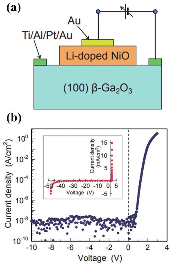
![(Color online) (a) Device schematic and (b) I–V characteristics of the sol-gel NiO/β-Ga2O3 heterojunction diode. Reproduced from Ref. [26]. Copyright 2016, The Japan Society of Applied Physics.](/richHtml/jos/2023/44/6/061802/jos_44_6_061802_f1.jpg)
Fig. 1. (Color online) (a) Device schematic and (b) I–V characteristics of the sol-gel NiO/β-Ga2O3 heterojunction diode. Reproduced from Ref. [26]. Copyright 2016, The Japan Society of Applied Physics.
![(Color online) (a) Schematic of the first kilovolt-class NiO/β-Ga2O3 heterojunction diode. The (b) forward and (c) reverse I–V characteristics of the devices. Reproduced from Ref. [27]. Copyright 2020, IEEE.](/richHtml/jos/2023/44/6/061802/jos_44_6_061802_f2.jpg)
Fig. 2. (Color online) (a) Schematic of the first kilovolt-class NiO/β-Ga2O3 heterojunction diode. The (b) forward and (c) reverse I–V characteristics of the devices. Reproduced from Ref. [27]. Copyright 2020, IEEE.
Fig. 3. (Color online) (a) XRD patterns of the sputtered NiO film on sapphire before and after annealing. (b) Cross-sectional HRTEM images of the NiO/β-Ga2O3 heterojunction interface. Reproduced from Ref. [48]. Copyright 2021, IEEE.
Fig. 4. (Color online) The energy band diagrams of the NiO/β-Ga2O3 heterojunctions at thermal equilibrium with different β-Ga2O3 substrate orientations. Reproduced from Ref. [47]. Copyright 2023, Elsevier B.V.
Fig. 5. (Color online) Band alignments of the NiO/β-Ga2O3 heterojunctions as a function of post-deposition annealing temperature. Reproduced from Ref. [57]. Copyright 2022, IOP Publishing Ltd.
Fig. 6. (Color online) (a) Temperature-dependent forward I–V characteristics and the fitting result with the interface recombination and trap-assisted tunneling current model. (b) ln(Jt0) versus temperature plot for the NiO/β-Ga2O3 heterojunction. Reproduced from Ref. [48]. Copyright 2021, IEEE.
Fig. 7. (Color online) Energy band diagrams of the NiO/β-Ga2O3 heterojunction p–n diode at a (a) low and (b) high forward bias. Reproduced from Ref. [48]. Copyright 2021, IEEE.
Fig. 8. (Color online) The milestones of the state-of-the-art NiO/β-Ga2O3 heterojunction based power devices. Reproduced from Refs. [27, 32, 33, 35]. Copyright 2021 and 2022, IEEE.
Fig. 9. (Color online) The (a) forward and (b) reverse I–V characteristics of the NiO/β-Ga2O3 heterojunction diodes with and without annealing. Reproduced from Ref. [66]. Copyright 2021, AIP Publishing.
Fig. 10. (Color online) (a) Cross-sectional schematic of the NiO/β-Ga2O3 heterojunction with small-angle bevel FP. The (b) forward and (c) reverse I–V characteristics of the devices. Reproduced from Ref. [25]. Copyright 2022, IEEE.
Fig. 11. (Color online) (a) Device schematic and (b) the reverse I–V characteristics of the double-layered NiO/β-Ga2O3 heterojunction diode. Reproduced from Ref. [68]. Copyright 2020, AIP Publishing.
Fig. 12. (Color online) (a) Simulated two-dimensional electric field distributions in the vicinity of the NiO and anode electrode at a reverse bias of 1000 V for the double-layered NiO/β-Ga2O3 HJD and (b) line profile of simulated electric field along the surface of the β-Ga2O3 drift layer for the HJD with varied W’ (W’ = Rp−NiO − Rp+NiO). Reproduced from Ref. [49]. Copyright 2022, IEEE.
Fig. 13. (Color online) (a) Device schematic and (b) the reverse I–V characteristics of the double-layered NiO/β-Ga2O3 heterojunction diode with varied thickness of the bottom NiO layer. Reproduced from Ref. [69]. Copyright 2022, AIP Publishing.
Fig. 14. (Color online) (a) Cross-sectional schematic of the NiO/β-Ga2O3 heterojunction diode with bevel mesa. The (b) forward and (c) reverse I–V characteristics of the devices. Reproduced from Ref. [70]. Copyright 2021, AIP Publishing.
Fig. 15. (Color online) (a) Cross-sectional schematic of the NiO/β-Ga2O3 heterojunction diode with double NiO layer and edge termination. The (b) forward and (c) reverse I–V characteristics of the devices. Reproduced from Ref. [62].
Fig. 16. (Color online) (a) Cross-sectional schematic of the NiO/β-Ga2O3 JBS diode. The (b) forward and (c) reverse I–V characteristics of the devices. Reproduced from Ref. [32]. Copyright 2021, IEEE.
Fig. 17. (Color online) (a) Cross-sectional schematic of the NiO/β-Ga2O3 JBS diode with fin structure. The (b) forward and (c) reverse I–V characteristics of the devices with different fin widths. Reproduced from Ref. [73]. Copyright 2021, AIP Publishing.
Fig. 18. (Color online) Cross-sectional schematic of (a) the NiO/β-Ga2O3 JFET and (b) the NiO/β-Ga2O3 JFET with recessed gate. Reproduced from Refs. [33, 81]. Copyright 2021 and 2022, IEEE.
Fig. 19. (Color online) (a) Schematic of β-Ga2O3 SBD with FLR. (b) Two-dimensional electric field distribution at a reverse bias of 1.89 kV for β-Ga2O3 SBD with FLR. Reproduced from Ref. [71]. Copyright 2021, AIP Publishing.
Fig. 20. (Color online) (a) Schematic of β-Ga2O3 SBD with NiO guard ring and FP termination. (b) Reverse I–V characteristics of β-Ga2O3 SBD without and with termination structure. Reproduced from Ref. [34]. Copyright 2022, AIP Publishing.
Fig. 21. (Color online) (a) 3-D schematic of the fabricated β-Ga2O3 SJ-equivalent MOSFET. (b) Measured ID–VD curves of the devices. (c) Reverse I–V characteristics of the devices. Reproduced from Ref. [35]. Copyright 2022, IEEE.
|
Table 1. Material properties of Ga2O3 and some competing semiconductors for power electronics.

Set citation alerts for the article
Please enter your email address


