Abstract
Beta gallium oxide (β-Ga2O3) has attracted significant attention for applications in power electronics due to its ultra-wide bandgap of ~ 4.8 eV and the large critical electric field of 8 MV/cm. These properties yield a high Baliga’s figures of merit (BFOM) of more than 3000. Though β-Ga2O3 possesses superior material properties, the lack of p-type doping is the main obstacle that hinders the development of β-Ga2O3-based power devices for commercial use. Constructing heterojunctions by employing other p-type materials has been proven to be a feasible solution to this issue. Nickel oxide (NiO) is the most promising candidate due to its wide band gap of 3.6–4.0 eV. So far, remarkable progress has been made in NiO/β-Ga2O3 heterojunction power devices. This review aims to summarize recent advances in the construction, characterization, and device performance of the NiO/β-Ga2O3 heterojunction power devices. The crystallinity, band structure, and carrier transport property of the sputtered NiO/β-Ga2O3 heterojunctions are discussed. Various device architectures, including the NiO/β-Ga2O3 heterojunction pn diodes (HJDs), junction barrier Schottky (JBS) diodes, and junction field effect transistors (JFET), as well as the edge terminations and super-junctions based on the NiO/β-Ga2O3 heterojunction, are described.1. Introduction
| Material | Si | GaAs | 4H-SiC | GaN | Diamond | Ga2O3 |
|---|
| Band gap (eV) | 1.1 | 1.43 | 3.25 | 3.4 | 5.5 | 4.6–4.9 |
| Critical electric field (MV/cm) | 0.3 | 0.4 | 2.5 | 3.3 | 10 | 8 |
| Electron mobility (cm2/(V·s)) | 1480 | 8400 | 1000 | 1250 | 2000 | 300 |
| Dielectric constant | 11.8 | 12.9 | 9.7 | 9 | 5.5 | 10 |
| Baliga FOM (
) | 1 | 14.7 | 317 | 846 | 24660 | \gt 3000 |
Table 1. Material properties of Ga2O3 and some competing semiconductors for power electronics.
Power devices have been widely used in switch control and high-power circuit driving, which play an essential role in multiple applications. With the fast development of electric automobiles, fifth-generation (5G) networks, and the internet of things (IoT), silicon material has generally reached its physical limit, and traditional silicon-based power electronics have been hard to satisfy the demand for many ultra-high power applications. Wide bandgap semiconductor materials such as silicon carbide (SiC), gallium nitride (GaN), diamond, and gallium oxide (Ga2O3) possess attractive properties and are considered potential candidates for next-generation power devices[1,2]. Among these, Ga2O3 has attracted significant attention due to its large critical electric field of 8 MV/cm and the high Baliga’s figure of merit (BFOM) of more than 3000[3-5]. The BFOM of Ga2O3 is much higher than that of Si, SiC, and GaN, indicating that Ga2O3-based devices can achieve higher breakdown voltage (BV) and lower specific on-resistance (Ron,sp) simultaneously.Table 1 compares the critical material parameters of several competing power electronics semiconductors. There are five phases of Ga2O3 labeled asα,β,γ,δ andε. The monoclinicβ-Ga2O3 is the most stable[6] and is commonly studied in fabricating power devices. Large-sizeβ-Ga2O3 bulk substrates can be synthesized by the low-coat melt-growth methods, such as floating zone (FZ) and edge-defined film-fed growth (EFG)[7,8], providing significant benefits for future mass production of electronic devices. Furthermore, high-quality homoepitaxy ofβ-Ga2O3 thin films can be realized by halide vapor phase epitaxy (HVPE), metal-organic chemical vapor deposition (MOCVD), and molecular beam epitaxy (MBE)[9-14].
N-type conduction inβ-Ga2O3 with a tunable doping concentration ranging from 1015 to 1019 cm−3 has been demonstrated by Si and Sn doping[8,15,16]. However, due to the large activation energy of acceptors and the large self-trapping energy of holes[17,18], p-type conduction inβ-Ga2O3 is proven difficult. The absence of p-typeβ-Ga2O3 is a major obstacle limiting the design ofβ-Ga2O3-based bipolar devices. A bipolar structure usually possesses low leakage current, high thermal stability, and good surge handling capability, which is much preferred over the unipolar configuration for power electronics. However, due to the lack of p-type doping, the studies ofβ-Ga2O3 power devices are mainly focused on unipolar devices such as Schottky barrier diodes (SBDs) and metal–oxide–semiconductor field effect transistors (MOSFETs)[19-22]. To overcome the obstacle, one possible solution is employing other p-type semiconductors and forming heterojunctions withβ-Ga2O3. Abundant investigations have been demonstrated onβ-Ga2O3 heterojunctions using various p-type semiconductors such as SiC, GaN, SnO, Cu2O, CuI, and NiO[23-30]. Among these, NiO is considered the most promising choice owing to its wide bandgap of 3.6-4.0 eV and controllable p-type doping with decent mobility[25-27,31]. Very recently, the first kilovolt-class NiO/β-Ga2O3 heterojunction pn diodes (HJDs) were successfully demonstrated by sputtering a p-NiO layer onβ-Ga2O3, which opened up a route toward future bipolar operation ofβ-Ga2O3 power electronics[27]. Following that, remarkable progress has been made by many researchers in improving the BFOM of the NiO/β-Ga2O3 HJDs. Furthermore, the NiO/β-Ga2O3 heterojunction has been adopted into other device architectures such as junction barrier Schottky diodes (JBSs)[32], junction field effect transistors (JFETs)[33] and edge termination structures[34,35].
This paper presents a detailed overview of the recent progress in NiO/β-Ga2O3 heterojunction power devices. Section 2 discusses the construction and characterization of the sputtered NiO/β-Ga2O3 heterojunction, focusing on its crystallinity, band structure, and carrier transport property. Section 3 and section 4 deal with the device technologies, including the NiO/β-Ga2O3 HJDs, JBSs, and JFETs, as well as the edge terminations and super-junctions based on the NiO/β-Ga2O3 heterojunction.
2. Construction and characterization of NiO/β-Ga2O3 heterojunction
2.1. Construction of high-voltage NiO/β-Ga2O3 heterojunction
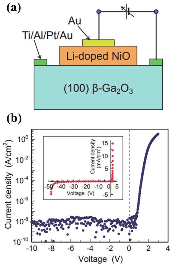
NiO thin films can be grown by several techniques such as sol-gel spin coating, radio frequency (RF) sputtering, pulsed laser deposition (PLD), atomic layer deposition (ALD), MBE, and thermal oxidation of Ni[31,36-42]. The initial study of NiO/β-Ga2O3 heterojunction was reported by Kokubunet al. in 2016[26]. A Li-doped NiO layer was grown on a 0.4-mm-thick (100)β-Ga2O3 single-crystal substrate (n = 5 × 1017 cm−3) by the sol-gel spin coating technique. The device schematic and current–voltage (I–V) characteristics of the sol-gel NiO/β-Ga2O3 HJD are shown inFig. 1. The device exhibited a high rectifying ratio of over 108 at ±3 V. However, the largeRon,sp of approximate 1 Ω·cm2 and low BV of 46 V indicated a suboptimal device performance for power applications. Tadjeret al.[41] reported the construction of NiO/β-Ga2O3 HJDs using sputtered and ALD-deposited NiO thin films. However, the fabricated devices showed either a very low forward current or a high reverse leakage current, which failed to satisfy the demand for power electronics. The NiO/β-Ga2O3 heterojunctions have also been fabricated by PLD for UV detection applications[43-46], yet the problem of high reverse current still existed.
![(Color online) (a) Device schematic and (b) I–V characteristics of the sol-gel NiO/β-Ga2O3 heterojunction diode. Reproduced from Ref. [26]. Copyright 2016, The Japan Society of Applied Physics.](/Images/icon/loading.gif)
Figure 1.(Color online) (a) Device schematic and (b) I–V characteristics of the sol-gel NiO/β-Ga2O3 heterojunction diode. Reproduced from Ref. [26]. Copyright 2016, The Japan Society of Applied Physics.
In 2020, the first kilovolt-class NiO/β-Ga2O3 HJD was successfully demonstrated by sputtering a p-NiO thin film onto an epitaxial n−-β-Ga2O3 drift layer[27], as shown inFig. 2. The NiO films were sputtered from a NiO target at room temperature and 3 mTorr pressure in a mixture of Ar/O2 ambient with RF power of 150 W. According to the Hall measurement, the hole concentration and hall mobility of the NiO were 1 ×1019 cm−3 and 0.24 cm2/(V·s), respectively. The fabricated NiO/β-Ga2O3 HJDs featured a high BV of over 1 kV with an ultra-low leakage current of below 1μA/cm2, representing a key milestone for the development of NiO/β-Ga2O3 heterojunction-based power devices. So far, RF sputtering has become the optimal method for depositing NiO onβ-Ga2O3, and continuous breakthrough has been achieved in the NiO/β-Ga2O3 heterojunction-based power devices.
Figure 2.(Color online) (a) Schematic of the first kilovolt-class NiO/β-Ga2O3 heterojunction diode. The (b) forward and (c) reverse I–V characteristics of the devices. Reproduced from Ref. [27]. Copyright 2020, IEEE.
2.2. Crystallinity and band structure of sputtered NiO/β-Ga2O3 heterojunction
X-ray diffraction (XRD) measurements and high-resolution transmission electron microscopy (HRTEM) observations have been used to investigate the crystallinity of the sputtered NiO/β-Ga2O3 heterojunction. Several reports have identified that the sputtered NiO films were polycrystalline even after a post-deposition annealing (PDA) process[25,27,47-49]. As shown inFig. 3(a), three diffraction peaks located at around 37.3°, 43.2° and 63.1° could be observed in the XRD patterns of the sputtered NiO films, which corresponded to the (111), (200), and (220) planes of NiO, respectively[48]. The HRTEM image inFig. 3(b) also revealed that the sputtered NiO film was generally polycrystalline with fine nanocrystalline grains and a seamless contact was formed at the NiO/β-Ga2O3 heterojunction interface. By comparing the XRD patterns and HRTEM images of the NiO films sputtered on (
), (001), and (010) orientedβ-Ga2O3 substrates, a very recent study pointed out that the crystallinity of sputtered NiO showed no strong dependency on theβ-Ga2O3 substrate orientations[47].
Figure 3.(Color online) (a) XRD patterns of the sputtered NiO film on sapphire before and after annealing. (b) Cross-sectional HRTEM images of the NiO/β-Ga2O3 heterojunction interface. Reproduced from Ref. [48]. Copyright 2021, IEEE.
It is known that the band structure of a heterojunction is crucial for device design and application. The band alignment of the heterojunction greatly influences its carrier transport properties. Thus it is essential to characterize the band offset at the heterojunction interface accurately. Gonget al.[50] reported a type-II band alignment of the sputtered NiO/β-Ga2O3 heterojunction with a valence band offset (VBO) of 3.60 eV and conduction band offset (CBO) of 2.68 eV. In comparison, Zhanget al.[45] reported a VBO value of 2.1 eV and CBO value of 0.9 eV for a similar sputtered NiO/β-Ga2O3 heterojunction. The band alignment of the sputtered NiO/β-Ga2O3 heterojunctions varies from each other, which could be determined by many factors, such as the strain, defects/vacancies, interfacial contamination, crystal orientation, and so on. Due to the crystalline anisotropy,β-Ga2O3 possesses anisotropic material properties and devices with different orientations show different performances[14,51-56]. The substrate orientation-dependent band alignment of the NiO/β-Ga2O3 heterojunctions was investigated by an X-ray photoelectron spectroscopy (XPS) analysis[47]. The VBO values of the NiO/β-Ga2O3 heterojunctions were extracted to be 2.12 ± 0.06, 2.44 ± 0.07, and 2.66 ± 0.07 eV for (
), (001) and (010)β-Ga2O3 substrates, respectively. The determined energy band diagrams of the NiO/β-Ga2O3 heterojunctions with differentβ-Ga2O3 orientations are shown inFig. 4. The influence of a PDA process on the band alignment of the NiO/β-Ga2O3 heterojunction was studied by Xiaet al.[57]. As shown inFig. 5, the band offsets monotonically increased while the bandgap of NiO decreased with the elevated annealing temperature up to 600 °C. The results also indicated a possible unstable performance of the NiO/β-Ga2O3 heterojunction device at high temperatures.
Figure 4.(Color online) The energy band diagrams of the NiO/β-Ga2O3 heterojunctions at thermal equilibrium with different β-Ga2O3 substrate orientations. Reproduced from Ref. [47]. Copyright 2023, Elsevier B.V.
Figure 5.(Color online) Band alignments of the NiO/β-Ga2O3 heterojunctions as a function of post-deposition annealing temperature. Reproduced from Ref. [57]. Copyright 2022, IOP Publishing Ltd.
2.3. Carrier transport mechanisms in the sputtered NiO/β-Ga2O3 heterojunction
Several groups have identified different forward conduction mechanisms rather than the conventional diffusion theory in the NiO/β-Ga2O3 heterojunction[48,50,58]. Due to the high barrier height against carriers in the type-II band structure, the diffusion and emission currents in the NiO/β-Ga2O3 heterojunction are negligible at a low forward bias. When the low forward bias is below 1.6 V, interface recombination has been revealed to be the dominant forward conduction mechanism of the NiO/β-Ga2O3 heterojunctions[48,50], in which the electrons and holes recombined once they meet at the heterojunction interface by overcoming the barrier of the depletion region. For an asymmetric heterojunction, the interface recombination current can be expressed as the following equation according to Grundmannet al.[59]
where
and
are the Boltzmann’s constant and the temperature,
and
are the dielectric constant and electron concentration of theβ-Ga2O3,
is the build-in potential in the NiO/β-Ga2O3 heterojunction, and
and
are the conductivities ofβ-Ga2O3 and NiO, respectively. The coefficient
or
represents the fast or low recombination occurring at the heterojunction interface. A near-zero
of ~0.008 was obtained for the sputtered NiO/β-Ga2O3 heterojunction at room temperature, indicating a relatively slow recombination. Given
fromC–V measurement, Gonget al.[50] also revealed a small
which decreased from 5.4 × 10⁻⁴ to 3.4 × 10⁻⁶ when the applied bias varied from
to
. Due to the large VBO (> 2 eV) of the NiO/β-Ga2O3 heterojunction, the holes in NiO can hardly be injected across the barrier at a low forward bias. Instead, the electrons contributed byβ-Ga2O3 recombine with the holes in the valence band of NiO through interfacial states, which forms the interface recombination current.
When the forward bias increased (>1.6 V), a trap-assisted multistep tunneling model became the dominant conduction mechanism in the NiO/β-Ga2O3 heterojunction[48]. The model can be described by the following equation[60,61]
where
,
is the doping concentration ofβ-Ga2O3,
is the number of steps of the tunneling, and
is a constant.Fig. 6(a) shows the fitting result of the two models, as mentioned above, with the experimental forwardI–V characteristics of the NiO/β-Ga2O3 heterojunction diodes at different temperatures, which exhibits a good agreement. The extracted
as a function of temperature showing good linearity further confirmed the multistep tunneling mechanism, as shown inFig. 6(b). It is speculated that the grain boundaries in the sputtered NiO films act as trap states[48] and facilitate electron tunneling[62]. In addition, according to the deep-level transient spectroscopy (DLTS) measurements carried out at a fixed reverse voltage of –6 V, a pulse filling voltage of +1 V, a pulse filling time of 0.02 ms, and a frequency of 1 Hz[63], an electron trap corresponded to the forward trap-assisted tunneling was observed in the spectra for the NiO/β-Ga2O3 heterojunction. This electron trap (ET) exhibited an energy level ofEC– 0.67 eV, which is related to Fe substituting for Ga on a tetrahedral site (FeGaI)[64]. It has been confirmed that Fe impurities unintentionally doped in the EFG bulkβ-Ga2O3 during the crystal growth[65], which might be the possible origination of theET.Fig. 7 shows the energy band diagrams and carrier dynamics of the NiO/β-Ga2O3 heterojunction.
Figure 6.(Color online) (a) Temperature-dependent forward I–V characteristics and the fitting result with the interface recombination and trap-assisted tunneling current model. (b) ln(Jt0) versus temperature plot for the NiO/β-Ga2O3 heterojunction. Reproduced from Ref. [48]. Copyright 2021, IEEE.
Figure 7.(Color online) Energy band diagrams of the NiO/β-Ga2O3 heterojunction p–n diode at a (a) low and (b) high forward bias. Reproduced from Ref. [48]. Copyright 2021, IEEE.
When the forward bias went beyond 3.5 V, a high-level injection phenomenon and corresponding conductivity modulation effect were observed[62]. This is because the energy band of NiO is pulled down at a very high forward bias, which leads to a significantly reduced hole barrier height at the Fermi tail; thus, the holes in NiO can travel across the heterojunction interface and diffuse intoβ-Ga2O3. DLTS spectra performed at the same condition in Ref. [63] but with frequency of 1200 Hz exhibited two positive peaks, which are the distinctive contribution by hole traps (HT). The detection of HT further confirmed the hole injection from p-NiO toβ-Ga2O3 in the heterojunction.
3. Device technology based on the NiO/β-Ga2O3 heterojunction
Possessing the advantages of low leakage current, high thermal stability, and good surge handling capability, bipolar power devices based on pn junctions have always attracted great attention, which promotes the blossoming of the NiO/β-Ga2O3 heterojunction-based power electronics. Very recently, a high BFOM of 13.21 GW/cm2 was successfully demonstrated in an 8-kV class sputtered NiO/β-Ga2O3 HJD, representing the highest BFOM value among all the reportedβ-Ga2O3 power devices[62]. Besides, high-performance JBSs[32] and JFETs[33] based on the NiO/β-Ga2O3 heterojunctions have been developed by several groups. Implementation of the NiO/β-Ga2O3 heterojunctions as edge terminations and super-junctions in various types ofβ-Ga2O3 power devices has been promised[34,35].Fig. 8 lists some milestones in developing state-of-the-art NiO/β-Ga2O3 heterojunction based power devices.
Figure 8.(Color online) The milestones of the state-of-the-art NiO/β-Ga2O3 heterojunction based power devices. Reproduced from Refs. [27, 32, 33, 35]. Copyright 2021 and 2022, IEEE.
NiO/β-Ga2O3 heterojunction diodes
3.1. NiO/β-Ga2O3 heterojunction diodes
As previously mentioned, the first 1 kV NiO/β-Ga2O3 HJDs[27] were fabricated using an 8-μm thick lightly doped (n = 4 × 1016 cm−3)β-Ga2O3 drift layer grown on a conductive (n = 2.6 × 1018 cm−3) (001) substrate with a 200-nm thick sputtered p-NiO layer (p = 1 × 1019 cm−3) on top. The device yielded a BV of 1059 V with an ultra-low leakage current of below 10−6 A/cm2 before breakdown and a lowRon,sp of 3.5 mΩ·cm2, leading to a BFOM of 0.32 GW/cm2. The results pave the way for developing high-performance bipolar power devices based on the NiO/β-Ga2O3 heterojunctions.
The trap states located within the sputtered NiO and at the heterojunction interface significantly affect the device performance of a NiO/β-Ga2O3 HJD. A PDA process has been proven as an effective method to improve the crystallinity of the sputtered NiO and reduce the defects density at the hetero-interface[48,49,66]. Moreover, the PDA process could also improve the metal-to-NiO Ohmic contact. Through a precisely controlled PDA process, Haoet al.[66] demonstrated the performance improved NiO/β-Ga2O3 HJDs. After annealing at 350 °C for 3 min in a nitrogen atmosphere, theRon,sp of the HJD was reduced from 5.4 to 4.1 mΩ·cm2 while the BV increased from 900 to 1630 V, leading to an improved BFOM from 0.16 to 0.65 GW/cm2 as shown inFig. 9. The ideality factor was extracted to be 3.02 and 1.27 for devices without and with annealing, and the calculated interface trap density (Nt) were about 1.04 × 10¹² and 1.33 × 10¹¹ eV−1, respectively.
Figure 9.(Color online) The (a) forward and (b) reverse I–V characteristics of the NiO/β-Ga2O3 heterojunction diodes with and without annealing. Reproduced from Ref. [66]. Copyright 2021, AIP Publishing.
Various field plate (FP) structures have been implemented in the NiO/β-Ga2O3 HJDs to manage the electric field. Gonget al.[67] reported a double-layered insulating FP structure. The first layer insulator was a 350-nm-thick SiNx layer deposited by plasma enhanced chemical vapor deposition (PECVD) at 300 °C and the second layer insulator was a 40-nm-thick Al2O3 layer grown by ALD at 300 °C. Subsequently, a 300 nm NiO layer with a length of field plate (LFP) of 10μm was deposited by RF sputtering. A PDA process was carried out at 300 °C in air for 1 h. The device demonstrated a BV of 1036 V and aRon,sp of 5.4 mΩ·cm2. A small-angle bevel FP structure was proposed for the NiO/β-Ga2O3 HJDs by Wanget al.[25], as shown inFig. 10. To realize the small-angel bevel FP, a 1-μm thick SiO2 was deposited by PECVD and dry etched using a photoresist mask formed by a variable-temperature photoresist reflow technique. The device featured a BV of up to 2410 V with a lowRon,sp of 1.12 mΩ·cm2, yielding a high BFOM of 5.18 GW/cm2. The bevel angle of the FP, the dielectric layer thickness, and the dimension of the FP are the critical parameters. With well-optimized parameters, this FP structure can offer great potential for fabricating high-voltageβ-Ga2O3 power devices.
Figure 10.(Color online) (a) Cross-sectional schematic of the NiO/β-Ga2O3 heterojunction with small-angle bevel FP. The (b) forward and (c) reverse I–V characteristics of the devices. Reproduced from Ref. [25]. Copyright 2022, IEEE.
Another approach to improve the performance of the NiO/β-Ga2O3 HJDs is using a double-layered NiO film[68]. As shown inFig. 11(a), the sputtered NiO film was composed of a 350-nm-thick lower-side lightly doped layer (p = 5.1 × 1017 cm−3) and a 100-nm-thick upper-side heavily doped layer (p = 3.6 × 1019 cm−3). Compared with the single-layered device (S2), the double-layered device (S1) demonstrated an enhanced BV from 0.94 to 1.86 kV, as shown inFig. 11(b). Liaoet al.[49] thoroughly optimized the double-layered NiO/β-Ga2O3 HJDs by performing both experimental study and technology computer-aided design (TCAD) simulation. It was revealed that the bottom lightly doped NiO layer could smoothen the electric field, while the upper heavily doped NiO layer can reduce theRon,sp by lowering the metal-to-NiO contact resistance. In addition, verified by the TCAD simulation, the electric field peak of the double-layered NiO/β-Ga2O3 HJDs located at the edge of the p+-NiO layer rather than the p−-NiO layer, and enlarging the dimension of the bottom p−-NiO layer can effectively suppress the electric field peak, as shown inFig. 12. The influence of the bottom NiO layer thickness was studied by Liet al.[69]. The device schematic is shown inFig. 13(a). The upper NiO layer (p = 2.6 × 1019 cm−3) was fixed at 10 nm, while the thickness of the bottom NiO layer (p = 3 × 1018 cm−3) ranged from 10 nm to 80 nm. The BV showed a negative correlation with the thickness of the bottom NiO layer, as shown inFig. 13(b).
Figure 11.(Color online) (a) Device schematic and (b) the reverse I–V characteristics of the double-layered NiO/β-Ga2O3 heterojunction diode. Reproduced from Ref. [68]. Copyright 2020, AIP Publishing.
Figure 12.(Color online) (a) Simulated two-dimensional electric field distributions in the vicinity of the NiO and anode electrode at a reverse bias of 1000 V for the double-layered NiO/β-Ga2O3 HJD and (b) line profile of simulated electric field along the surface of the β-Ga2O3 drift layer for the HJD with varied W’ (W’ = Rp−NiO − Rp+NiO). Reproduced from Ref. [49]. Copyright 2022, IEEE.
Figure 13.(Color online) (a) Device schematic and (b) the reverse I–V characteristics of the double-layered NiO/β-Ga2O3 heterojunction diode with varied thickness of the bottom NiO layer. Reproduced from Ref. [69]. Copyright 2022, AIP Publishing.
Zhouet al.[70] demonstrated a novel beveled-mesa NiO/β-Ga2O3 HJD, as shown inFig. 14. By precisely adjusting the gap between the mask andβ-Ga2O3 wafer as well as the declination angle of the NiO target with respect to the substrate surface normal, the double-layered NiO film with a small beveled angle was formed. The fabricated large-area (1 mm2) HJDs performed a lowRon,sp of 2.26 mΩ·cm2 and a high BV of 2.04 kV, leading to a BFOM of 1.84 GW/cm2. A remarkable BV of 8.32 kV was achieved in the NiO/β-Ga2O3 HJD[62] by employing the double-layered NiO structure and advanced edge terminations of an FP and an Mg-implanted guard ring. Ion implantation in the device periphery to form a high-resistivity region can effectively relieve the electric field crowing effect and improve the breakdown voltage in power devices.Fig. 15 shows the schematic andI–V characteristics of the device. A lowRon,sp of 5.24 mΩ·cm2 was obtained for the 8.32 kV HJD, and the BFOM of 13.21 GW/cm2 was the highest value among all the reportedβ-Ga2O3 power devices so far.
Figure 14.(Color online) (a) Cross-sectional schematic of the NiO/β-Ga2O3 heterojunction diode with bevel mesa. The (b) forward and (c) reverse I–V characteristics of the devices. Reproduced from Ref. [70]. Copyright 2021, AIP Publishing.
Figure 15.(Color online) (a) Cross-sectional schematic of the NiO/β-Ga2O3 heterojunction diode with double NiO layer and edge termination. The (b) forward and (c) reverse I–V characteristics of the devices. Reproduced from Ref. [62].
3.2. NiO/β-Ga2O3 heterojunction JBS
Schottky barrier diodes (SBDs) possess properties of low turn-on voltage and fast switching speed. Meanwhile, p–n diodes have the advantages of low leakage current and good surge handling capability. The JBS devices can combine the advantages of SBDs and p–n diodes.
The first NiO/β-Ga2O3 heterojunction JBS was demonstrated by Lvet al.[32].Fig. 16 shows the schematic and theI–V characteristics of the JBS device. The NiO layer (p = 1 × 1018 cm−3) with a thickness of 60 nm was formed by thermally oxidizing Ni metal. The fabricated JBS showed a lowVon of ~1 V, slightly higher than the reference SBD (~0.7 V). The BV of the JBS was as high as 1715 V, far superior to that of the reference SBD (655 V). However, these JBSs suffered from a huge reverse leakage current under a high electric field, and the leakage mechanism was determined to be a Pool-Frenkel (PF) emission, which refers to the electric-field-enhanced thermal excitation of electrons from a trapped state into a continuum of electronic states[71]. According to the Arrhenius plots of the reverse leakage current vs. 1000/T measured at various reverse biases, the emission barrier height was determined to beEC – 0.72 eV below the conduction band, which is consistent with the energy level of gallium vacancies (VGa)[72]. It indicated that in such a JBS structure, the NiO/β-Ga2O3 heterojunction failed to suppress the reverse leakage current through the Schottky contact region. To address this issue, the NiO/β-Ga2O3 heterojunction JBSs with etched fin structures were developed[73]. The fin structures on theβ-Ga2O3 drift layer were firstly formed by reactive ion etching (RIE), and then the trenches between the fins were filled with sputtered p-NiO, as schematically shown inFig. 17(a). With the fin structures, the pn heterojunction depleted laterally at the reverse bias, which lowered the density of free carriers left in theβ-Ga2O3 channel; thus, the fin structures would help to suppress the leakage current through the Schottky contact region. Three JBSs with different fin widths were fabricated. TheVon andRon,sp of the JBSs were measured to be 1.7 V/2.45 mΩ·cm2, 1.5 V/1.94 mΩ·cm2, and 1.45 V/1.91 mΩ·cm2, for the fin width of 1.5, 3, and 5μm, respectively. Since the forwardI–V characteristics of a JBS should be mainly determined by its Schottky contact region, the device had a greater proportion of Schottky contact area showed a closer value ofVon andRon,sp to an SBD. However, the measured BV of the JBSs did not show a strong dependence on the fin width. Though the reverse leakage current was partially suppressed by using the fin structures, the dry etching process produced high-density deep-level traps at theβ-Ga2O3 surface, which might introduce excess leakage current[74,75]. A post-etching treatment process would be helpful to remove the defects from the etchedβ-Ga2O3 surface, for example, surface treatment using a hot tetramethylammonium hydroxide (TMAH) solution[76]. At present, high reverse leakage current is still the remaining issue that hinders the development of the NiO/β-Ga2O3 heterojunction JBSs.
Figure 16.(Color online) (a) Cross-sectional schematic of the NiO/β-Ga2O3 JBS diode. The (b) forward and (c) reverse I–V characteristics of the devices. Reproduced from Ref. [32]. Copyright 2021, IEEE.
Figure 17.(Color online) (a) Cross-sectional schematic of the NiO/β-Ga2O3 JBS diode with fin structure. The (b) forward and (c) reverse I–V characteristics of the devices with different fin widths. Reproduced from Ref. [73]. Copyright 2021, AIP Publishing.
3.3. NiO/β-Ga2O3 heterojunction JFET
The development of lateralβ-Ga2O3 field-effect transistors (FETs) has achieved remarkable progress[77-80]. However, the reported device performance is still far from the projected material limitation ofβ-Ga2O3. The channel doping level and thickness must be carefully designed to ensure an effective channel pinch-off in a lateral FET and obtain a good balance between theRon,sp and BV. Theβ-Ga2O3 JFETs based on the NiO/β-Ga2O3 heterojunctions have been proposed by Wanget al. for the first time[33], as shown inFig. 18(a). The employed p-NiO gate provided a vertical depletion to theβ-Ga2O3 channel and facilitated the channel pinch-off. Therefore, a relatively thicker channel and higher channel doping concentration could be used in the device to minimize theRon,sp without sacrificing the BV. On the other hand, the lateral depletion of the heterojunction in the channel could help smooth the electric field at the drain-side-gate-edge and boost the BV of the JFETs. The fabricated devices exhibited a lowRon,sp of 3.19 mΩ·cm2 and a high BV of 1115 V, yielding a BFOM of 0.39 GW/cm2. Using a gate-recessed architecture, a normally-off operation has been realized in the NiO/β-Ga2O3 heterojunction JFETs[81]. As schematically shown inFig. 18(b), the 200 nm channel was recessed down to 80 nm in the gate region by an inductively coupled plasma (ICP) etching process, and a 50 nm p-NiO gate was sputtered. A positive threshold voltage (Vth) of +0.9 V was achieved.
Figure 18.(Color online) Cross-sectional schematic of (a) the NiO/β-Ga2O3 JFET and (b) the NiO/β-Ga2O3 JFET with recessed gate. Reproduced from Refs. [33, 81]. Copyright 2021 and 2022, IEEE.
4. NiO/β-Ga2O3 heterojunction-based edge terminations and super-junctions
Various edge termination techniques, such as FP[19,82], ion-implanted GR[20,83,84], and thermally oxidized terminations[85], have been developed to relieve the electric field crowding and enhance the BV of theβ-Ga2O3 power device.
The field limiting ring (FLR) using p–n junctions is an effective structure to suppress the electric field peak at the device edge, which is commonly used in SiC power devices[86]. An improved BV has been reported inβ-Ga2O3 SBDs by adopting a NiO/β-Ga2O3 heterojunction-based FLR[71], as shown inFig. 19(a). Compared to the device without the FLR, the average BV was increased from 0.43 to 0.75 kV. A TCAD simulation was carried out to investigate the influence of the NiO/β-Ga2O3 heterojunction FLR on the electric field distribution of the devices under a reverse bias. As shown inFig. 19(b), the electric field spread out into the FLR structures, and the crowding of the electric field at the device edge was effectively mitigated.
Figure 19.(Color online) (a) Schematic of β-Ga2O3 SBD with FLR. (b) Two-dimensional electric field distribution at a reverse bias of 1.89 kV for β-Ga2O3 SBD with FLR. Reproduced from Ref. [71]. Copyright 2021, AIP Publishing.
The p-NiO guard ring has also been employed inβ-Ga2O3 SBDs[34]. As shown inFig. 20, a 300-nm trench was etched in theβ-Ga2O3 drift layer and subsequently filled with sputtered p-NiO (p = 1 × 1018 cm−3) to construct the guard ring. The SBDs showed an improved BV of 1130 V by introducing the p-NiO guard ring compared to a BV of 300 V for SBDs without the guard ring. By further implementation of an FP structure, the BV was boosted to 1860 V.
Figure 20.(Color online) (a) Schematic of β-Ga2O3 SBD with NiO guard ring and FP termination. (b) Reverse I–V characteristics of β-Ga2O3 SBD without and with termination structure. Reproduced from Ref. [34]. Copyright 2022, AIP Publishing.
Super-junction (SJ) is a promising technique to manage the electric field in power devices[87-90], which has been successfully commercialized in Si devices[91,92] and also introduced in GaN and SiC devices[93-95]. With an alternative arrangement of p-type and n-type stripes, the SJ structure can uniform the electric field distribution in the drift layer, relying on the charge balance principle[96]. Wanget al.[35] demonstrated a novel super-junctionβ-Ga2O3 MOSFET based on the NiO/β-Ga2O3 heterojunctions, as shown inFig. 21. Trenches in theβ-Ga2O3 drift layer were formed using ICP etching and then filled with sputtered NiO (p = 1 × 1018 cm−3). Compared with a co-fabricated conventional MOSFET, the SJ MOSFETs exhibited an improved BFOM by 4.86 times.
Figure 21.(Color online) (a) 3-D schematic of the fabricated β-Ga2O3 SJ-equivalent MOSFET. (b) Measured ID–VD curves of the devices. (c) Reverse I–V characteristics of the devices. Reproduced from Ref. [35]. Copyright 2022, IEEE.
5. Summary and prospects
Still at the very early stage of development, the NiO/β-Ga2O3 heterojunction has shown great potential for application inβ-Ga2O3 power electronics. In this review, we summarized the state-of-the-art device technology and development of NiO/β-Ga2O3 heterojunction power devices. Despite the encouraging progress, some crucial issues still exist for practical application.
First, developing high-qualityβ-Ga2O3 material, including both the substrate and the epi film, is the cornerstone for future improvement of the power devices. The unintentional impurities, defects, and dislocations within theβ-Ga2O3 crystal can significantly affect the device performances regarding leakage current, electrical conductivity, device reliability, etc.
The device structure optimization is essential to further enhance the device voltage blocking capability. As mentioned, the double NiO layers, FP structures, and ion-implanted GRs are all feasible solutions. Still, further improvements in the details of these structures remain. For example, the dielectric layer’s materials, thickness, and deposition process are critical factors for an FP structure. As for the ion-implanted GRs, more investigation is needed on different implanted ions, the profiles of the implanted region, and the post-implantation annealing conditions.
Trap states at the NiO/β-Ga2O3 heterojunction interface can cause large hysteresis and excess reverse leakage current. As mentioned, a PDA process is an effective method to improve the heterojunction interface quality. However, the forward conduction can be degraded by annealing since the hole concentration of the NiO layer decreases. Surface treatment using solutions or a plasma process is also a practical method to remove the defects at theβ-Ga2O3 surface and realize a high-quality hetero-interface.
Device reliability is very important for the commercial application of the NiO/β-Ga2O3 heterojunction power devices, especially at high temperatures. The sputtered NiO layer usually faces a thermal stability issue, whose hole concentration usually reduces at high temperatures. The reliability verifications for the NiO/β-Ga2O3 heterojunction devices are still lacking and awaiting future exploration.
References
[1] X She, A Q Huang, Ó Lucía et al. Review of silicon carbide power devices and their applications. IEEE Trans Ind Electron, 64, 8193(2017).
[2] E A Jones, F F Wang, D Costinett. Review of commercial GaN power devices and GaN-based converter design challenges. IEEE J Emerg Sel Top Power Electron, 4, 707(2016).
[3] A K Saikumar, S D Nehate, K B Sundaram. Review—RF sputtered films of Ga2O3. ECS J Solid State Sci Technol, 8, Q3064(2019).
[4] S J Pearton, J C Yang, P H Cary et al. A review of Ga2O3 materials, processing, and devices. Appl Phys Rev, 5, 011301(2018).
[5] H Zhou, J C Zhang, C F Zhang et al. A review of the most recent progresses of state-of-art gallium oxide power devices. J Semicond, 40, 011803(2019).
[6] S Yoshioka, H Hayashi, A Kuwabara et al. Structures and energetics of Ga2O3 polymorphs. J Phys: Condens Matter, 19, 346211(2007).
[7] E G Víllora, K Shimamura, Y Yoshikawa et al. Large-size β-Ga2O3 single crystals and wafers. J Cryst Growth, 270, 420(2004).
[8] A Kuramata, K Koshi, S Watanabe et al. High-quality β-Ga2O3 single crystals grown by edge-defined film-fed growth. Jpn J Appl Phys, 55, 1202A2(2016).
[9] F Alema, Y W Zhang, A Osinsky et al. Low temperature electron mobility exceeding 104 cm2/V s in MOCVD grown β-Ga2O3. APL Mater, 7, 121110(2019).
[10] Y W Zhang, F Alema, A Mauze et al. MOCVD grown epitaxial β-Ga2O3 thin film with an electron mobility of 176 cm2/V s at room temperature. APL Mater, 7, 022506(2018).
[11] Y P Chen, X C Xia, H W Liang et al. Growth pressure controlled nucleation epitaxy of pure phase ε- and β-Ga2O3 films on Al2O3 via metal–organic chemical vapor deposition. Cryst Growth Des, 18, 1147(2018).
[12] S A Kukushkin, V I Nikolaev, A V Osipov et al. Epitaxial gallium oxide on a SiC/Si substrate. Phys Solid State, 58, 1876(2016).
[13] H L Wei, Z W Chen, Z P Wu et al. Epitaxial growth and characterization of CuGa2O4 films by laser molecular beam epitaxy. AIP Adv, 7, 115216(2017).
[14] K Sasaki, M Higashiwaki, A Kuramata et al. MBE grown Ga2O3 and its power device applications. J Cryst Growth, 378, 591(2013).
[15] C Joishi, S Rafique, Z B Xia et al. Low-pressure CVD-grown β-Ga2O3 bevel-field-plated Schottky barrier diodes. Appl Phys Express, 11, 031101(2018).
[16] M Baldini, M Albrecht, A Fiedler et al. Si- and Sn-doped homoepitaxial β-Ga2O3 layers grown by MOVPE on (010)-oriented substrates. ECS J Solid State Sci Technol, 6, Q3040(2016).
[17] J B Varley, A Janotti, C Franchini et al. Role of self-trapping in luminescence and p-type conductivity of wide-band-gap oxides. Phys Rev B, 85, 081109(2012).
[18] J L Lyons. A survey of acceptor dopants for β. Semicond Sci Technol, 33, 05LT02(2018).
[19] J C Yang, M H Xian, P Carey et al. Vertical geometry 33.2 A, 4.8 MW cm2 Ga2O3 field-plated Schottky rectifier arrays. Appl Phys Lett, 114, 232106(2019).
[20] H Zhou, Q L Yan, J C Zhang et al. High-performance vertical β-Ga2O3 Schottky barrier diode with implanted edge termination. IEEE Electron Device Lett, 40, 1788(2019).
[21] W S Li, K Nomoto, Z Y Hu et al. Field-plated Ga2O3 trench Schottky barrier diodes with a BV2/Ron, sp of up to 0.95 GW/cm2. IEEE Electron Device Lett, 41, 107(2020).
[22] Z A Jian, S Mohanty, E Ahmadi. Switching performance analysis of 3.5 kV Ga2O3 power FinFETs. IEEE Trans Electron Devices, 68, 672(2021).
[23] S Nakagomi, K Hiratsuka, Y Kakuda et al. Beta-gallium oxide/SiC heterojunction diodes with high rectification ratios. ECS J Solid State Sci Technol, 6, Q3030(2016).
[24] Y C Zhang, Y F Li, Z Z Wang et al. Investigation of β-Ga2O3 films and β-Ga2O3/GaN heterostructures grown by metal organic chemical vapor deposition. Sci China Phys Mech Astron, 63, 117311(2020).
[25] Y G Wang, H H Gong, Y J Lv et al. 2.41 kV vertical P-NiO/n-Ga2O3 heterojunction diodes with a record Baliga’s figure-of-merit of 5.18 GW/cm2. IEEE Trans Power Electron, 37, 3743(2022).
[26] Y Kokubun, S Kubo, S Nakagomi. All-oxide p–n heterojunction diodes comprising p-type NiO and n-type β-Ga2O3. Appl Phys Express, 9, 091101(2016).
[27] X Lu, X D Zhou, H X Jiang et al. 1-kV sputtered p-NiO/n-Ga2O3 heterojunction diodes with an ultra-low leakage current below 1 μA/cm2. IEEE Electron Device Lett, 41, 449(2020).
[28] T Watahiki, Y Yuda, A Furukawa et al. Heterojunction p-Cu2O/n-Ga2O3 diode with high breakdown voltage. Appl Phys Lett, 111, 222104(2017).
[29] M Budde, D Splith, P Mazzolini et al. SnO/β-Ga2O3 vertical pn heterojunction diodes. Appl Phys Lett, 117, 252106(2020).
[30] J C Gallagher, A D Koehler, M J Tadjer et al. Demonstration of CuI as a P–N heterojunction to β. Appl Phys Express, 12, 104005(2019).
[31] H L Chen, Y M Lu, W S Hwang. Characterization of sputtered NiO thin films. Surf Coat Technol, 198, 138(2005).
[32] Y J Lv, Y G Wang, X C Fu et al. Demonstration of β-Ga2O3 junction barrier Schottky diodes with a Baliga’s figure of merit of 0.85 GW/cm2 or a 5A/700 V handling capabilities. IEEE Trans Power Electron, 36, 6179(2021).
[33] C L Wang, H H Gong, W N Lei et al. Demonstration of the p-NiOx/n-Ga2O3 heterojunction gate FETs and diodes with BV2/Ron, sp figures of merit of 0.39 GW/cm2 and 1.38 GW/cm2. IEEE Electron Device Lett, 42, 485(2021).
[34] Q L Yan, H H Gong, H Zhou et al. Low density of interface trap states and temperature dependence study of Ga2O3 Schottky barrier diode with p-NiOx termination. Appl Phys Lett, 120, 092106(2022).
[35] Y B Wang, H H Gong, X L Jia et al. Demonstration of β-Ga2O3 superjunction-equivalent MOSFETs. IEEE Trans Electron Devices, 69, 2203(2022).
[36] Y Wang, Q Z Qin. A nanocrystalline NiO thin-film electrode prepared by pulsed laser ablation for Li-ion batteries. J Electrochem Soc, 149, A873(2002).
[37] M Jlassi, I Sta, M Hajji et al. Optical and electrical properties of nickel oxide thin films synthesized by sol–gel spin coating. Mater Sci Semicond Process, 21, 7(2014).
[38] J H Park, J Seo, S Park et al. Efficient CH3NH3PbI3 perovskite solar cells employing nanostructured p-type NiO electrode formed by a pulsed laser deposition. Adv Mater, 27, 4013(2015).
[39] I Hotový, D Búc, Š Haščík et al. Characterization of NiO thin films deposited by reactive sputtering. Vacuum, 50, 41(1998).
[40] M Budde, T Remmele, C Tschammer et al. Plasma-assisted molecular beam epitaxy of NiO on GaN(00.1). J Appl Phys, 127, 015306(2020).
[41] M J Tadjer, L E Luna, E Cleveland et al. Fabrication and characterization of β-Ga2O3 heterojunction rectifiers. ECS Trans, 85, 21(2018).
[42] F Hajakbari. Characterization of nanocrystalline nickel oxide thin films prepared at different thermal oxidation temperatures. J Nanostruct Chem, 10, 97(2020).
[43] M I Pintor-Monroy, D Barrera, B L Murillo-Borjas et al. Tunable electrical and optical properties of nickel oxide (NiOx) thin films for fully transparent NiOx-Ga2O3 p-n junction diodes. ACS Appl Mater Interfaces, 10, 38159(2018).
[44] P Schlupp, D Splith, H von Wenckstern et al. Electrical properties of vertical p-NiO/n-Ga2O3 and p-ZnCo2O4/n-Ga2O3 pn-heterodiodes. Phys Status Solidi A, 216, 1800729(2019).
[45] J Y Zhang, S B Han, M Y Cui et al. Fabrication and interfacial electronic structure of wide bandgap NiO and Ga2O3 p–n heterojunction. ACS Appl Electron Mater, 2, 456(2020).
[46] K H Li, N Alfaraj, C H Kang et al. Deep-ultraviolet photodetection using single-crystalline β-Ga2O3/NiO heterojunctions. ACS Appl Mater Interfaces, 11, 35095(2019).
[47] Y X Deng, Z Q Yang, T L Xu et al. Band alignment and electrical properties of NiO/β-Ga2O3 heterojunctions with different β-Ga2O3 orientations. Appl Surf Sci, 622, 156917(2023).
[48] H X Luo, X D Zhou, Z M Chen et al. Fabrication and characterization of high-voltage NiO/β-Ga2O3 heterojunction power diodes. IEEE Trans Electron Devices, 68, 3991(2021).
[49] C Liao, X Lu, T L Xu et al. Optimization of NiO/β-Ga2O3 heterojunction diodes for high-power application. IEEE Trans Electron Devices, 69, 5722(2022).
[50] H H Gong, X H Chen, Y Xu et al. Band alignment and interface recombination in NiO/β-Ga2O3 type-II p-n heterojunctions. IEEE Trans Electron Devices, 67, 3341(2020).
[51] Z Guo, A Verma, X F Wu et al. Anisotropic thermal conductivity in single crystal β-gallium oxide. Appl Phys Lett, 106, 111909(2015).
[52] M H Wong, K Sasaki, A Kuramata et al. Electron channel mobility in silicon-doped Ga2O3 MOSFETs with a resistive buffer layer. Jpn J Appl Phys, 55, 1202B9(2016).
[53] S Jang, S Jung, K Beers et al. A comparative study of wet etching and contacts on (
2¯01
) and (010) oriented β-Ga2O3. J Alloys Compd, 731, 118(2018).
[54] K Zhang, Z W Xu, J L Zhao et al. Anisotropies of angle-resolved polarized Raman response identifying in low miller index β-Ga2O3 single crystal. Appl Surf Sci, 581, 152426(2022).
[55] R Yatskiv, S Tiagulskyi, J Grym. Influence of crystallographic orientation on Schottky barrier formation in gallium oxide. J Electron Mater, 49, 5133(2020).
[56] H Q Fu, H Chen, X Q Huang et al. A comparative study on the electrical properties of vertical (
2¯01
) and (010) β-Ga2O3 Schottky barrier diodes on EFG single-crystal substrates. IEEE Trans Electron Devices, 65, 3507(2018).
[57] X Y Xia, J S Li, C C Chiang et al. Annealing temperature dependence of band alignment of NiO/β-Ga2O3. J Phys D: Appl Phys, 55, 385105(2022).
[58] Z P Wang, H H Gong, C X Meng et al. Majority and minority carrier traps in NiO/β-Ga2O3 p-n heterojunction diode. IEEE Trans Electron Devices, 69, 981(2022).
[59] M Grundmann, R Karsthof, H von Wenckstern. Interface recombination current in type II heterostructure bipolar diodes. ACS Appl Mater Interfaces, 6, 14785(2014).
[60] A R Riben, D L Feucht. Electrical transport in nGe-pGaAs heterojunctions. Int J Electron, 20, 583(1966).
[61] A R Riben, D L Feucht. nGe–pGaAs heterojunctions. Solid State Electron, 9, 1055(1966).
[62] J C Zhang, P F Dong, K Dang et al. Ultra-wide bandgap semiconductor Ga2O3 power diodes. Nat Commun, 13, 3900(2022).
[63] Z P Wang, H H Gong, X X Yu et al. Trap-mediated bipolar charge transport in NiO/Ga2O3 p+-n heterojunction power diodes. Sci China Mater, 66, 1157(2022).
[64] C Zimmermann, Y K Frodason, A W Barnard et al. Ti- and Fe-related charge transition levels in β-Ga2O3. Appl Phys Lett, 116, 072101(2020).
[65] M E Ingebrigtsen, J B Varley, A Y Kuznetsov et al. Iron and intrinsic deep level states in Ga2O3. Appl Phys Lett, 112, 042104(2018).
[66] W B Hao, Q M He, K Zhou et al. Low defect density and small I − V curve hysteresis in NiO/β-Ga2O3 pn diode with a high PFOM of 0.65 GW/cm2. Appl Phys Lett, 118, 043501(2021).
[67] H H Gong, X X Yu, Y Xu et al. Vertical field-plated NiO/Ga2O3 heterojunction power diodes. 2021 5th IEEE Electron Devices Technology & Manufacturing Conference (EDTM), 1(2021).
[68] H H Gong, X H Chen, Y Xu et al. A 1.86-kV double-layered NiO/β-Ga2O3 vertical p–n heterojunction diode. Appl Phys Lett, 117, 022104(2020).
[69] J S Li, C C Chiang, X Y Xia et al. Demonstration of 4.7 kV breakdown voltage in NiO/β-Ga2O3 vertical rectifiers. Appl Phys Lett, 121, 042105(2022).
[70] F Zhou, H H Gong, Z P Wang et al. Over 1.8 GW/cm2 beveled-mesa NiO/β-Ga2O3 heterojunction diode with 800 V/10 A nanosecond switching capability. Appl Phys Lett, 119, 262103(2021).
[71] H H Gong, X X Yu, Y Xu et al. β-Ga2O3 vertical heterojunction barrier Schottky diodes terminated with p-NiO field limiting rings. Appl Phys Lett, 118, 202102(2021).
[72] C De Santi, M Fregolent, M Buffolo et al. Carrier capture kinetics, deep levels, and isolation properties of β-Ga2O3 Schottky-barrier diodes damaged by nitrogen implantation. Appl Phys Lett, 117, 262108(2020).
[73] Q L Yan, H H Gong, J C Zhang et al. β-Ga2O3 hetero-junction barrier Schottky diode with reverse leakage current modulation and BV2/Ron,sp value of 0.93 GW/cm2. Appl Phys Lett, 118, 122102(2021).
[74] A Y Polyakov, I H Lee, N B Smirnov et al. Defects at the surface of β-Ga2O3 produced by Ar plasma exposure. APL Mater, 7, 061102(2019).
[75] G Alfieri, A Mihaila, P Godignon et al. Deep level study of chlorine-based dry etched β-Ga2O3. J Appl Phys, 130, 025701(2021).
[76] X Lu, T L Xu, Y X Deng et al. Performance-enhanced NiO/β-Ga2O3 heterojunction diodes fabricated on an etched β-Ga2O3 surface. Appl Surf Sci, 597, 153587(2022).
[77] Y J Lv, X Y Zhou, S B Long et al. Lateral source field-plated β-Ga2O3 MOSFET with recorded breakdown voltage of 2360 V and low specific on-resistance of 560 mΩ cm2. Semicond Sci Technol, 34, 11LT02(2019).
[78] J K Mun, K Cho, W Chang et al. Editors' choice—2.32 kV breakdown voltage lateral β-Ga2O3 MOSFETs with source-connected field plate. ECS J Solid State Sci Technol, 8, Q3079(2019).
[79] K Tetzner, E Bahat Treidel, O Hilt et al. Lateral 1.8 kV β-Ga2O3 MOSFET with 155 MW/cm2 power figure of merit. IEEE Electron Device Lett, 40, 1503(2019).
[80] Y J Lv, H Y Liu, X Y Zhou et al. Lateral β-Ga2O3 MOSFETs with high power figure of merit of 277 MW/cm2. IEEE Electron Device Lett, 41, 537(2020).
[81] X Z Zhou, Q Liu, W B Hao et al. Normally-off β-Ga2O3 power heterojunction field-effect-transistor realized by p-NiO and recessed-gate. 2022 IEEE 34th International Symposium on Power Semiconductor Devices and ICs (ISPSD), 101(2022).
[82] K Konishi, K Goto, H Murakami et al. 1-kV vertical Ga2O3 field-plated Schottky barrier diodes. Appl Phys Lett, 110, 103506(2017).
[83] Y N Zhang, J C Zhang, Z Q Feng et al. Impact of implanted edge termination on vertical β-Ga2O3 Schottky barrier diodes under OFF-state stressing. IEEE Trans Electron Devices, 67, 3948(2020).
[84] Y Y Gao, A Li, Q Feng et al. High-voltage β-Ga2O3 Schottky diode with argon-implanted edge termination. Nanoscale Res Lett, 14, 8(2019).
[85] Y G Wang, Y J Lv, S B Long et al. High-voltage (-201) β-Ga2O3 vertical Schottky barrier diode with thermally-oxidized termination. IEEE Electron Device Lett, 41, 131(2020).
[86] T Hirao, H Onose, Y S Kan et al. Edge termination with enhanced field-limiting rings insensitive to surface charge for high-voltage SiC power devices. IEEE Trans Electron Devices, 67, 2850(2020).
[87] T Fujihira. Theory of semiconductor superjunction devices. Jpn J Appl Phys, 36, 6254(1997).
[88] G Deboy, N Marz, J P Stengl et al. A new generation of high voltage MOSFETs breaks the limit line of silicon. International Electron Devices Meeting, 683(1998).
[89] L Lorenz, G Deboy, A Knapp et al. COOLMOS/sup TM/-a new milestone in high voltage power MOS. 11th International Symposium on Power Semiconductor Devices and ICs, 3(1999).
[90] F Udrea, G Deboy, T Fujihira. Superjunction power devices, history, development, and future prospects. IEEE Trans Electron Devices, 64, 713(2017).
[91] S G Nassif-Khalil, C A T Salama. Super-junction LDMOST on a silicon-on-sapphire substrate. IEEE Trans Electron Devices, 50, 1385(2003).
[92] B X Duan, Z Cao, X Yuan et al. New superjunction LDMOS breaking silicon limit by electric field modulation of buffered step doping. IEEE Electron Device Lett, 36, 47(2015).
[93] M Xiao, R Z Zhang, D Dong et al. Design and simulation of GaN superjunction transistors with 2-DEG channels and fin channels. IEEE J Emerg Sel Top Power Electron, 7, 1475(2019).
[94] X Q Zhong, B Z Wang, J Wang et al. Experimental demonstration and analysis of a 1.35-kV 0.92-m Ω·cm2 SiC superjunction Schottky diode. IEEE Trans Electron Devices, 65, 1458(2018).
[95] A Nakajima, Y Sumida, M H Dhyani et al. GaN-based super heterojunction field effect transistors using the polarization junction concept. IEEE Electron Device Lett, 32, 542(2011).
[96] H Wang, E Napoli, F Udrea. Breakdown voltage for superjunction power devices with charge imbalance: An analytical model valid for both punch through and non punch through devices. IEEE Trans Electron Devices, 56, 3175(2009).