
Minmin Rong, Yijun Zhang, Shiman Li, Gangcheng Jiao, Weixin Liu, Ziheng Wang, Zhaoxin Shu, Yunsheng Qian. InGaAs Surface Cleaning Based on Scanning Focused XPS Technique[J]. Acta Optica Sinica, 2021, 41(5): 0516004
- Acta Optica Sinica
- Vol. 41, Issue 5, 0516004 (2021)
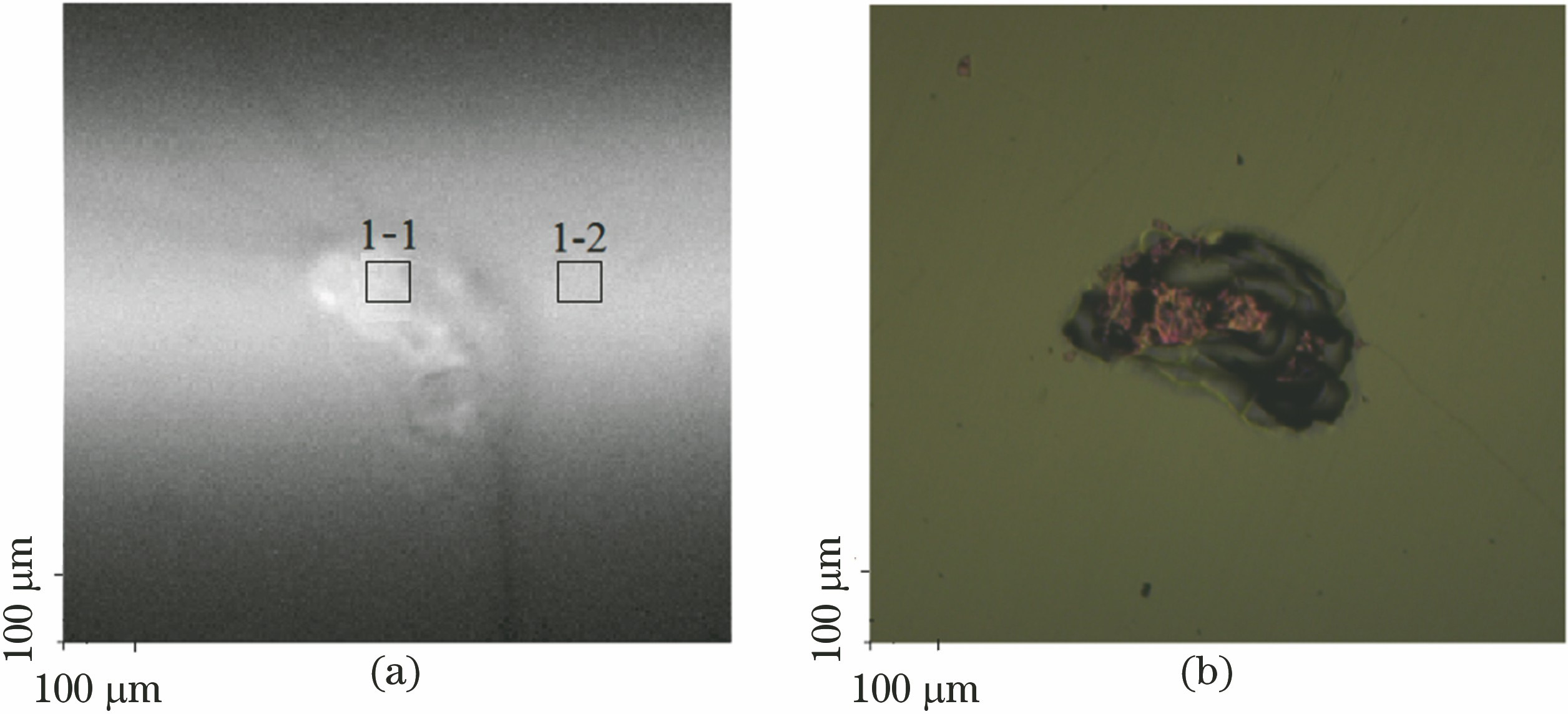
Fig. 1. Surface SXI and optical microscope images for sample 1. (a) SXI image; (b) optical microscope image
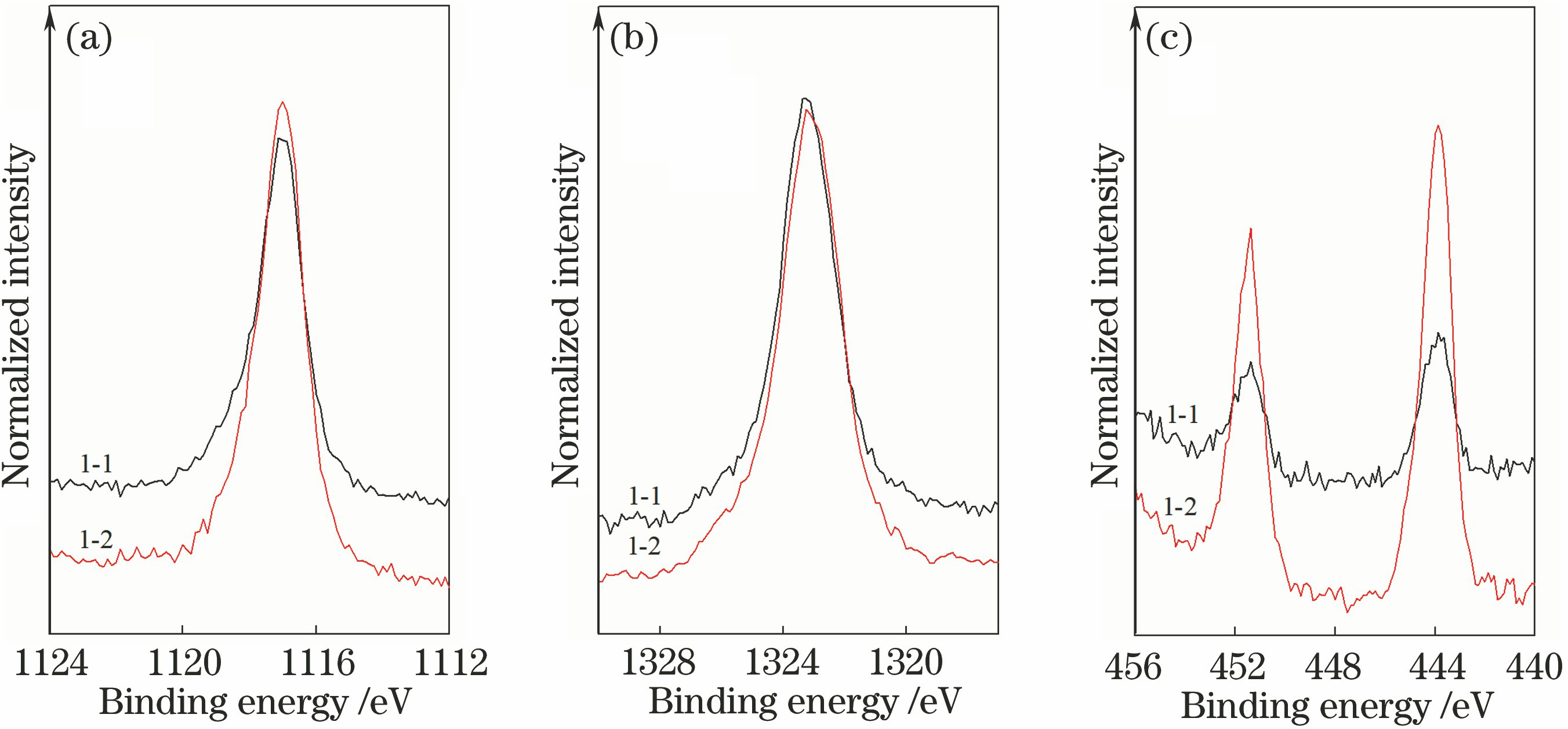
Fig. 2. XPS spectra of elements in micro-areas 1-1 and 1-2. (a) Ga2p3; (b) As2p3; (c) In3d
Fig. 3. XPS fitted spectra of Ga2p3 for different samples. (a) Uncleaned sample; (b) sample 1; (c) sample 2; (d) sample 3
Fig. 4. XPS fitted spectra of As2p3 for different samples. (a) Uncleaned sample; (b) sample 1; (c) sample 2; (d) sample 3
Fig. 5. XPS fitted spectra of In3d for different samples. (a) Uncleaned sample; (b) sample 1; (c) sample 2; (d) sample 3
Fig. 6. XPS spectra of C1s and O1s for different samples. (a) C1s; (b) O1s
Fig. 7. XPS spectra of C1s and O1s for different sample after different cleaning steps. (a) C1s; (b) O1s
Fig. 8. XPS fitted spectra of Ga2p3 for sample 4 after different cleaning steps. (a) Uncleaning; (b) UV-ozone cleaning; (c) degreasing cleaning; (d) etching based on HCl and IPA mixed solution
Fig. 9. XPS fitted spectra of As2p3 for sample 4 after different cleaning steps. (a) Uncleaning; (b) UV-ozone cleaning; (c) degreasing cleaning; (d) etching based on HCl and IPA mixed solution
Fig. 10. XPS fitted spectra of In3d for sample 4 after different cleaning steps. (a) Uncleaning; (b) UV-ozone cleaning; (c) degreasing cleaning; (d) etching based on HCl and IPA mixed solution
|
Table 1. XPS fitted peak ratios of surface micro-area elements for different samplesunit: %
|
Table 2. XPS fitted peak ratios of surface micro-area elements for different samples after different cleaning stepsunit: %

Set citation alerts for the article
Please enter your email address
© Copyright 2018-2021 | Chinese Laser Press. All Rights Reserved 沪ICP备15018463号-20