
Haiou Li, Xin Zhang, Guoping Guo. Controlling spins in silicon quantum dots[J]. Journal of Semiconductors, 2020, 41(7): 070402
- Journal of Semiconductors
- Vol. 41, Issue 7, 070402 (2020)
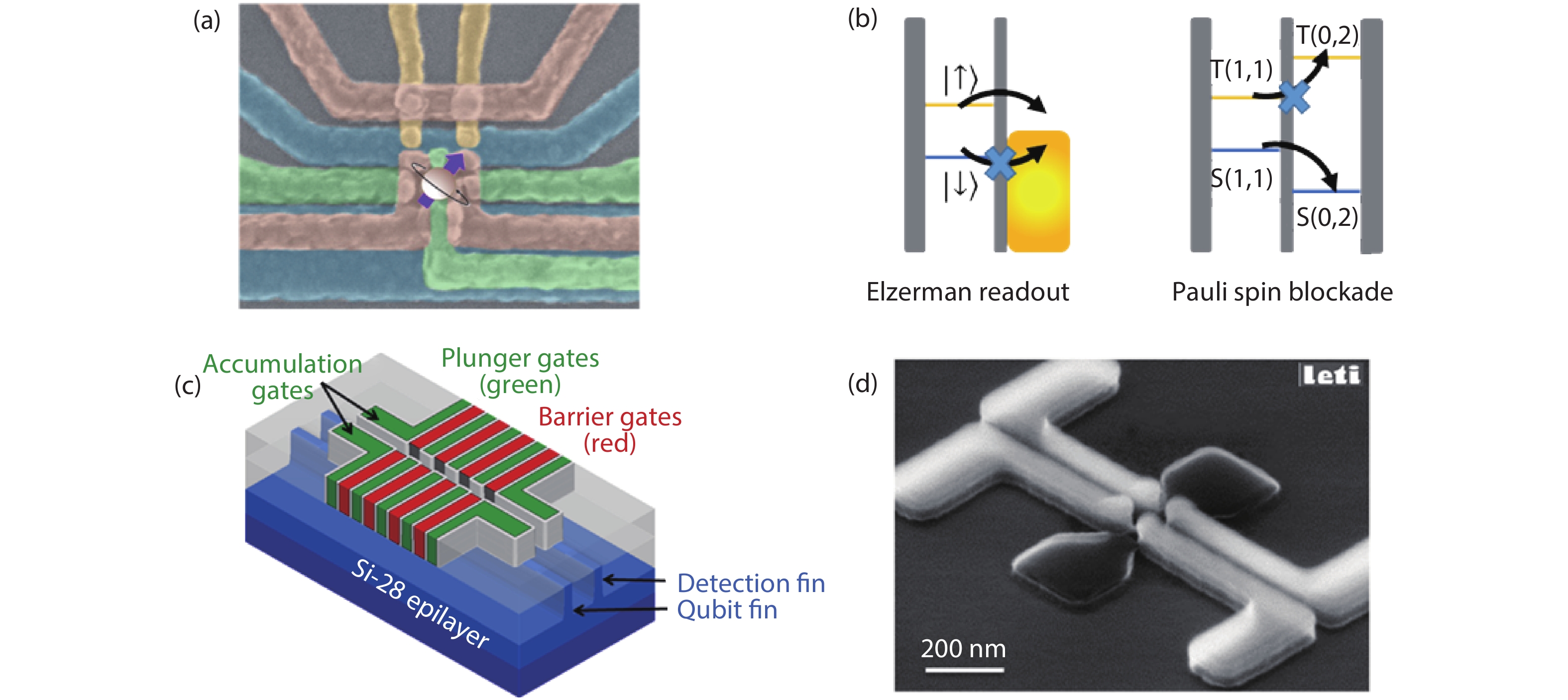
Fig. 1. (Color online) (a) False-color scanning electron microscopy (SEM) image of an overlapping-gate Si QD. (b) Energy level arrangement for Elezerman readout and Pauli spin blockade readout. (c) Dual nested gate integration of Si QDs using fin field-effect transistor (FinFET) technology. (d) SEM image of a two dimensional array of Si QDs using fully-depleted silicon-on-insulator transistor (FD-SOI) technology.
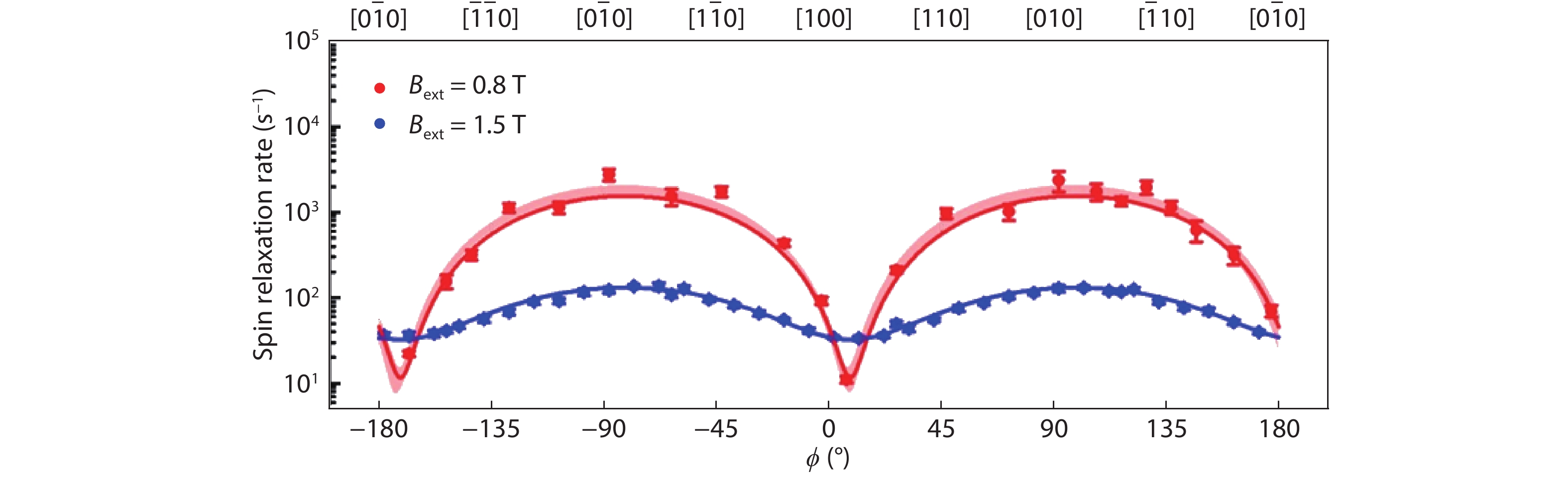
Fig. 2. (Color online) Angle dependence of the relaxation rate measured with different magnetic field strengths.

Set citation alerts for the article
Please enter your email address
© Copyright 2018-2021 | Chinese Laser Press. All Rights Reserved 沪ICP备15018463号-20