
Xian Zhang, Xiaodong Cao, Xuelian Zhang. A 16-bit 1 MSPS SAR ADC with foreground calibration and residual voltage shift strategy[J]. Journal of Semiconductors, 2020, 41(12): 122401
- Journal of Semiconductors
- Vol. 41, Issue 12, 122401 (2020)
Abstract
1. Introduction
With the increasing application of biological and wireless sensing techniques, the 16-bit 1 MSPS SAR ADC has a huge market with big potential and wide prospects. Due to the rapid development of CMOS process technology, SAR ADC has become a hot spot in the ADC design field[
The second part of this paper introduces the ADC system and detailed circuit implementation. The RS strategy and RS-based dither are described in the third part. The on-chip all-digital foreground weights calibration technique is illustrated in detail in the fourth part. The layout and simulation results are shown in the fifth part.
2. System and circuits implementation
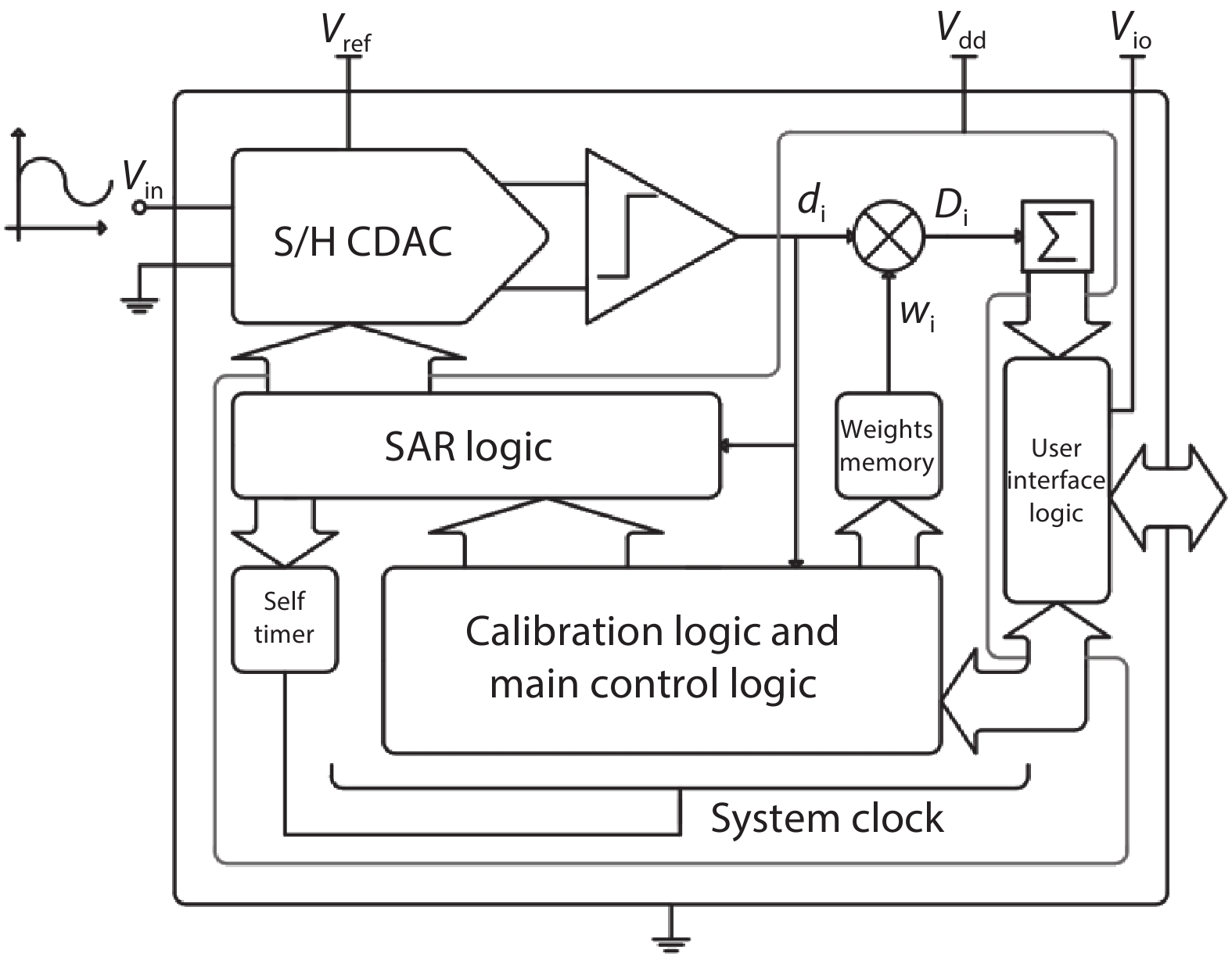
The system architecture of the all-digital foreground self-calibration 16-bit 1 MSPS SAR ADC is shown in Fig. 1, which consists of a carefully designed sample-and-hold capacitor digital-to-analog converter (S/H CDAC), a high-performance comparator, and an innovative digital logic circuit. The digital logic circuit consists of a SAR logic circuit, a calibration logic circuit, and a serial peripheral interface (SPI) circuit. The analog part and digital part of the SAR ADC can cooperate seamlessly as a whole. To meet the requirements of wide input voltage range, low power consumption, ease-of-use and small area, three power supplies are used in this design. The reference voltage (
![]()
Figure 1.The ADC system architecture.
2.1. High-performance self-timer comparator
The conversion result depends on the accuracy of the comparator, which is influenced by many factors, such as area, power consumption, noise, offset, and settling time[
![]()
Figure 2.Comparator block diagram.
In the designed SAR ADC, an auto-zero[
![]()
Figure 3.Preamplifier.
![]()
Figure 4.Multiphase clock of the self-timer.
2.2. S/H CDAC
Ref. [9] elaborates on the advantages of a split CDAC, and the three-segment CDAC applied in Ref. [8] is reported to have great advantages in SAR ADCs with 12 bits or more. The proposed design adopts a differential three-segment CDAC, which effectively optimizes the area and setting time of the capacitor. The half structure is shown in Fig. 5. Considering
![]()
Figure 5.The schematic of half CDAC.
All of the capacitors except
2.3. SAR control logic
Fig. 6(a) illustrates the simplified SAR control logic circuits[
![]()
Figure 6.(a) Control logic circuit. (b) High-segment MUX switch circuit.
During the conversion process, SELn outputs high potentials one by one to control the corresponding MUX switch circuit to set and latch the comparison results. The high-segment MUX switches are implemented, as shown in Fig. 6(b). When preparing for the on-chip calibration, the MU1 module is set to its initial value (1 or 0). The initial values, the setting state, and the comparison results are saved in the latch that consists of inverters I1 and I2. During the sampling phase, M1 and M2 are turned off while T1 is turned on. At the end of the sampling phase, the input signal is saved in the top plate of the sampling capacitors. Delay circuits B1 and B2 are used for generating dead time to avoid simultaneous conduction of M1 and M2.
3. Residual voltage shift strategy and RS-based dither
3.1. Residual voltage shift strategy
The conversion errors are induced by clock jitter, comparator misjudgment, setting errors, and reference voltage noises. The conversion fault tolerance can be effectively improved by adding appropriate redundant bits in the CDAC[
![]()
Figure 7.(a) Weights of a 6 phase SAR ADC and the start phase. (b) Residual voltage curves of P and N curves.
Three redundant bits and an RS bit are added to improve the fault tolerance of the 6 phase SAR ADC. Fig. 7(a) shows the start phase of the conversion process, and the 4th bit of the 6 phase SAR ADC is selected to work as RS bit. In the Fig. 7(a), 1 represents that this bit is set to
![]()
Figure 8.(Color online) (a) Simulation residual voltage with third bit error. (b) Simulation residual voltage with second bit error.
Fig. 9 shows the relationship between the number of the RS bits and the noise floor level with10 kHz sine signal input. The noise floor level can be optimized effectively by adding an appropriate RS bit during the conversion process.
![]()
Figure 9.Simulated noise floor level versus number of RS bits.
The four residual voltage curves of the same input signal are shown in Fig. 10(a). The error resident curve 1 is the nonideal case with RS strategy and the error happens in the 13th bit. The error resident curve 2 is the case with misjudgment due to the insufficient residual voltage and the error happens in the 9th bit. After point P1, the error residual curve 1 emerges an erroneous rise because an error decision is produced in 13th bit. The RS bits help the error residual curve 1 to drop to the ideal residual voltage curve when the 12R bit decision is over. This additional falling portion is the pre-offset voltage of the 12th bit. These additional drops help the residual curve return to a correct range that is close to the ideal residual curve. Actually, the error resident curve 1 returns back to a correct range when the 11th bit trial is complete, which means the previous mentioned error is resolved. The error residual curve 2 shows the residual curve without RS strategy. The error residual curve 2 shows a continuous drop after the error point P2, but the continuous drop still cannot correct the residual voltage. In fact, the error like P2 may occur not only in the 9th bit but also in the 9R bit. The 9th weight is the same as the weight of 9R bit. So, the location of the residual curve remains unchanged when the 9th bit is compared with 9R bit. Though the residual curve remains unchanged, the weight capacitors are still charged and discharged with the potential errors.
![]()
Figure 10.(Color online) (a) Residual voltage curves. (b) Start phase and RS bits.
The first function of the RS strategy is used to correct the error caused by the insufficient rise of the residual curve during the setting phase. The second function of the RS strategy is used to dynamically change the residual voltage to reduce the comparator decision error. During the conversion process, the irrevocable mistake decision emerges easily in the first previous bits because the first previous bits decision time and setting time are shorter than the later bits. Since the decision error caused by the insufficient rise of the residual curve is proportional to weight error, an earlier insufficient rise error may cause a larger conversion error. The position and weight of redundant bits are obtained after detailed analysis, so better results can be achieved when the RS bit is added to the redundant bit. On the other hand, the situation that the comparator repeats the decision of the small and indistinguishable input voltage is reduced when the RS bit is added to the redundant bit. The start-up state after adding the RS bit is shown in Fig. 10(b). Fig. 11 shows the INL and DNL with/without RS bits. It can be seen that the RS strategy reduces INL errors and DNL errors effectively in the unideal environment.
![]()
Figure 11.(Color online) Simulated INL and DNL with/without RS strategy.
3.2. RS-based dither
Nonlinearity error caused by capacitance mismatch of the CDAC degrades SNDR and SFDR, because the error appears as spurs of ADC output spectrum[
An all-analog dither technique is proposed in this paper. The second RS bit, third RS bit, and fourth RS bit are used to work as the dither bits in this design. The pseudo-random sequence drives the dither bits to affect the transfer function. In the conversion process, dither bits can be set to the RS bits value when the previous RS dither bit is settled to the comparison result. The conversion results are influenced by the RS dither bits. The RS dither bits are used like normal bits throughout the conversion process, so the digital result does not need to subtract the weights of dither bits. The non-ideal factors such as noise and comparator offset are added in the simulation. As shown in Fig. 12, it can be seen that the noise floor of the SAR ADC with RS-based dither is better than that without RS-based dither.
![]()
Figure 12.(Color online) Simulated noise floor with/without RS-based dither.
4. Calibration
Refs. [8, 22, 23] employ an all-digital foreground calibration technique, which uses the less significant bits to measure more significant bits. The 5th bit is the first calibration bit in this design. The detailed calibration process of P and N terminals of the 5th bit is as follows. Firstly, the P terminal of the 5th bit is set to
![]()
Figure 13.(a) Calibration start phase of the P bits (b) Calibration start phase of the N bits.
Affected by the noise, the single calibration result may be hard to meet the requirements of a 16-bit resolution. Therefore, it is necessary to make multiple measurements and take the average as the final result to reduce the influence of noise. Multiple measurements are made for each weight to reduce the effects of the noise[
![]()
Figure 14.(Color online) Simulated noise floor level versus average number.
In practice, the mismatch causes a mismatch voltage of CDAC between the P and N terminals, and when the mismatch voltage is greater than the sum of weights of 5th bits to LSB, the calibration process fails. Therefore, an auto-balance strategy is added in the second segment of the CDAC to remove the mismatch voltage in this design. The simplified automatic balance CDAC is shown in Fig. 15. The auto-balance strategy adjusts the mismatch voltage between P and N terminals of the CDAC to less than 1 LSB before the calibration process.
![]()
Figure 15.Auto-balance circuit.
In the self-measurement calibration technique, the digital weights of lower six bits are specified, so the calibrated digital weights fluctuate with the capacitance mismatch. This phenomenon causes serious gain errors. Therefore, the automatic gain adjustment is required to reduce the gain error. Eq. (6) gives the calculation method of the automatic gain adjustment. When the weights are calibrated, the ADC measures
In this SAR ADC, a total of 28 data (24 bits) are generated during the calibration process, including weight data of each bit and automatic gain adjustment data. Figs. 16 and 17 show the INL, DNL, and the noise floor level of this SAR ADC with/without being calibrated. The simulation results reveal that auto-balance, self-measurement weight calibration and automatic gain adjustment strategies well correct INL and DNL errors, and improve the noise floor performance. During the calibration process, the operating temperature is the key factor that affects the accuracy of the calibration. Fig. 18 shows the relationship between the average absolute value of the weight errors and the temperature.
![]()
Figure 16.(Color online) Simulated results of INL and DNL with/without calibration.
![]()
Figure 17.(Color online) Simulated results of noise floor with/without calibration.
![]()
Figure 18.Simulated results of the average absolute value of weight errors versus temperature.
5. Layout and result
The final performance of the SAR ADC can be directly affected by the layout. The layout of the SAR ADC needs to be carefully designed, such as the interference of the comparator, self-timer, digital logic and CDAC. The self-timer and the clock trees of digital logic generate significant jitters on the power supply. The random jitters are coupled into the output of the CDAC through the bulk, parasitic capacitors, and comparator circuits. When the outputs of the CDAC are contaminated, the performances of the SAR ADC are degraded severely. So, the interference barrier structures are necessary for the layout. On the other hand, the transmission distances of key signals need to be shorter. Therefore, the layout needs to tradeoff between the interference and the signal transmission distance. The final layout is shown in Fig. 19. The switch array of the CDAC in the layout is used as a barrier to shield against the interference of digital logic and self-timer. The comparator is placed near the output of the CDAC. The layout skills are employed to improve the design performances and the simulation results prove that the design performance is guaranteed by a reasonable layout. The post-layout simulation result is shown in Fig. 20. At the end of the conversion, the residual voltage is less than 20 µV.
![]()
Figure 19.(Color online) The layout of the 16bit 1MSPS SAR ADC with on-chip calibration.
![]()
Figure 20.(Color online) The post-layout simulated result of the residual voltage.
The final simulation results are given in Table 2. Table 2 shows the comparison between the recent excellent medium-speed high-precision SAR ADCs and this design. This work has a great market in cheap applications of medium-speed high-precision SAR ADCs.
6. Conclusion
A 16-bit 1MSPS SAR ADC with digital foreground calibration is developed in this paper. In this design, the self-measurement weight calibration, auto-balance, and automatic gain strategies are employed to guarantee that the SAR ADC achieves a 16-bit resolution. RS strategy and RS-based dither strategy are presented for optimizing the conversion stability effectively. A high-performance self-timer auto-zero comparator is applied to lower the power cost and optimize the decision time. The ADC is implemented with 0.25 μm CMOS process and the simulation results show the ADC meets 16-bit 1MSPS requirements.
References
[1] W Kim, H K Hong, Y J Roh et al. A 0.6 V 12 b 10 MS/s low-noise asynchronous SAR-assisted time-interleaved SAR (SATI-SAR) ADC. IEEE J Solid-State Circuits, 51, 1826(2016).
[2] A Shikata, R Sekimoto, T Kuroda et al. A 0.5 V 1.1 MS/sec 6.3 fJ/conversion-Step SAR-ADC with tri-level comparator in 40 nm CMOS. IEEE J Solid-State Circuits, 47, 1022(2012).
[3] P Harpe, E Cantatore, A van Roermund. A 10b/12b 40 kS/s SAR ADC with data-driven noise reduction achieving up to 10.1b ENOB at 2.2 fJ/conversion-step. IEEE J Solid-State Circuits, 48, 3011(2013).
[4] P Nuzzo, F De Bernardinis, P Terreni et al. Noise analysis of regenerative comparators for reconfigurable ADC architectures. IEEE Trans Circuits Syst I, 55, 1441(2008).
[5] B Verbruggen, J Tsouhlarakis, T Yamamoto et al. A 60 dB SNDR 35 MS/s SAR ADC with comparator-noise-based stochastic residue estimation. IEEE J Solid-State Circuits, 50, 2002(2015).
[6] J Y Zhong, Y Zhu, C H Chan et al. A 12b 180MS/s 0.068mm2 with full-calibration-integrated pipelined-SAR ADC. IEEE Trans Circuits Syst I, 64, 1684(2017).
[7] N Verma, A P Chandrakasan. An ultra low energy 12-bit rate-resolution scalable SAR ADC for wireless sensor nodes. IEEE J Solid-State Circuits, 42, 1196(2007).
[8] J H Shen, A Shikata, L D Fernando et al. A 16-bit 16-MS/s SAR ADC with on-chip calibration in 55-nm CMOS. IEEE J Solid-State Circuits, 53, 1149(2018).
[9] Y Chen, X Zhu, H Tamura et al. Split capacitor DAC mismatch calibration in successive approximation ADC. IEICE Trans Electron, 93, 295(2010).
[10] J A McNeill, K Y Chan, M C W Coln et al. All-digital background calibration of a successive approximation ADC using the “split ADC” architecture. IEEE Trans Circuits Syst I, 58, 2355(2011).
[11]
[12] J L McCreary, P R Gray. All-MOS charge redistribution analog-to-digital conversion techniques. I. IEEE J Solid-State Circuits, 10, 371(1975).
[13] P J Harpe, C Zhou, Y Bi et al. A 26 W 8 bit 10 MS/s asynchronous SAR ADC for low energy radios. IEEE J Solid-State Circuits, 46, 1585(2011).
[14]
[15] C C Liu, S J Chang, G Y Huang et al. A 10-bit 50-MS/s SAR ADC with a monotonic capacitor switching procedure. IEEE J Solid-State Circuits, 45, 731(2010).
[16] P Harpe, Y Zhang, G Dolmans et al. A 7-to-10b 0-to-4MS/s flexible SAR ADC with 6.5-to-16fJ/conversion-step. 2012 IEEE International Solid-State Circuits Conference, 472(2012).
[17] M J Seo, Y J Roh, D J Chang et al. A reusable code-based SAR ADC design with CDAC compiler and synthesizable analog building blocks. IEEE Trans Circuits Syst II, 65, 1904(2018).
[18]
[19] T Miki, T Morie, K Matsukawa et al. A 4.2 mW 50 MS/s 13 bit CMOS SAR ADC With SNR and SFDR enhancement techniques. IEEE J Solid-State Circuits, 50, 1372(2015).
[20] C P Hurrell, C Lyden, D Laing et al. An 18 b 12.5 MS/s ADC with 93 dB SNR. IEEE J Solid-State Circuits, 45, 2647(2010).
[21] M F Wagdy, M Goff. Linearizing average transfer characteristics of ideal ADC's via analog and digital dither. IEEE Trans Instrum Meas, 43, 146(1994).
[22]
[23]
[24] M Maddox, B Z Chen, M Coln et al. A 16 bit linear passive-charge-sharing SAR ADC in 55nm CMOS. 2016 IEEE Asian Solid-State Circuits Conf (A-SSCC), 153(2016).

Set citation alerts for the article
Please enter your email address
© Copyright 2018-2021 | Chinese Laser Press. All Rights Reserved 沪ICP备15018463号-20