[1] W L Barnes, A Dereux, T W Ebbesen. Surface plasmon subwavelength optics. Nature, 424, 824(2003).
[2] H Lu, X Liu, G Wang et al. Tunable high-channel-count bandpass plasmonic filters based on an analogue of electromagnetically induced transparency. Nanotechnology, 23, 444003(2012).
[3] H Q Wang, J B Yang, J J Zhang et al. Tunable band-stop plasmonic waveguide filter with symmetrical multiple-teeth-shaped structure. Opt Lett, 41, 1233(2016).
[4] P B Johnson, R W Christy. Optical constants of the noble metals. Phys Rev B, 6, 4370(1972).
[5] P R West, S Ishii, G V Naik et al. Searching for better plasmonic materials. Laser Photonics Rev, 4, 795(2010).
[6] W S Cai, U K Chettiar, A V Kildishev et al. Optical cloaking with metamaterials. Nat Photonics, 1, 224(2007).
[7]
[8]
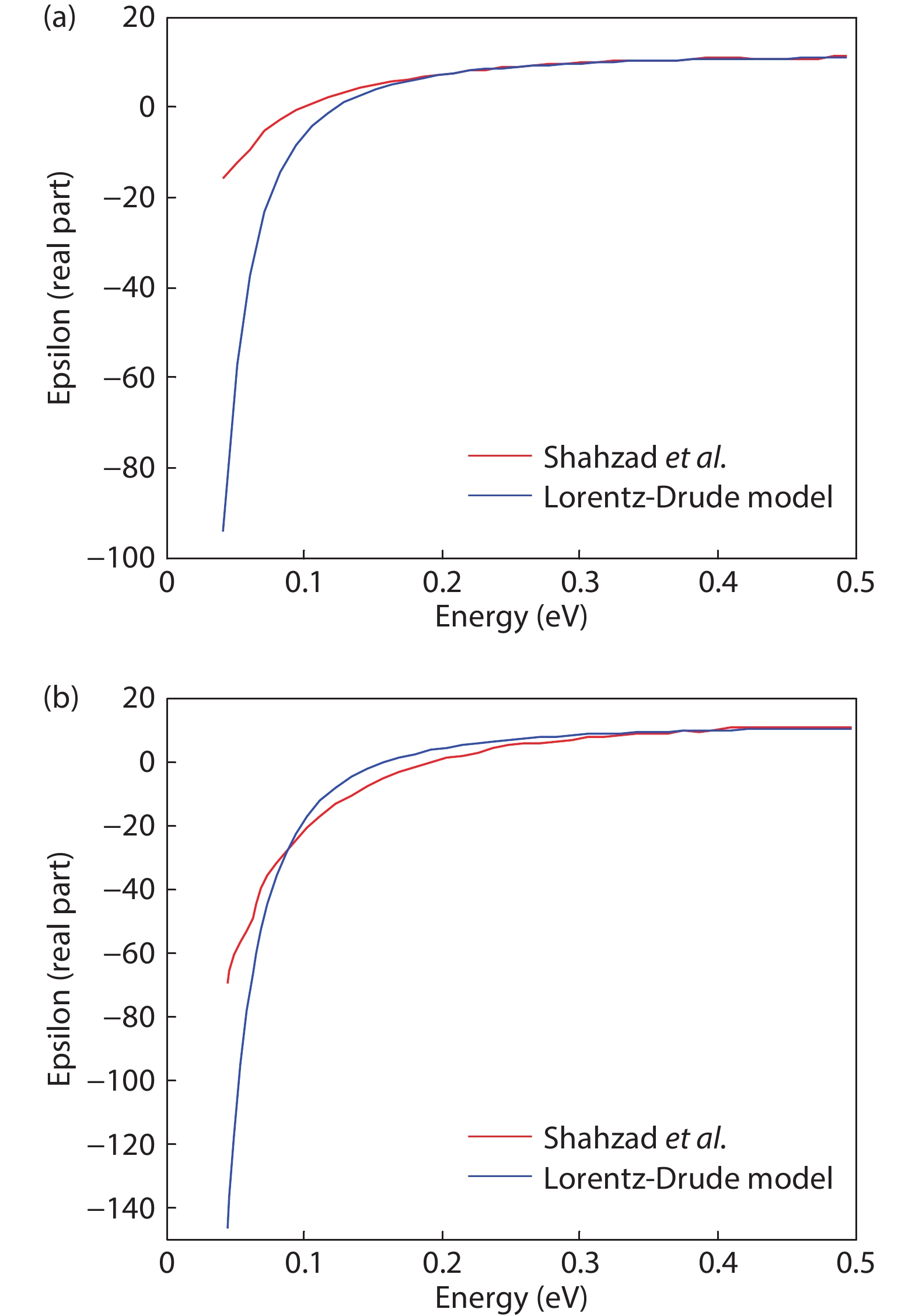
[9] M Shahzad, G Medhi, R E Peale et al. Infrared surface plasmons on heavily doped silicon. J Appl Phys, 110, 123105(2011).
[10] D Linaschke, N Schilling, I Dani et al. Highly n-doped surfaces on n-type silicon wafers by laser-chemical processes. Energy Procedia, 55, 247(2014).
[11] I Mizushima, A Murakoshi, M Watanabe et al. Hole generation without annealing in high dose boron implanted silicon: Heavy doping by B12 icosahedron as a double acceptor. Jpn J Appl Phys, 33, 404(1994).
[12] L Viña, M Cardona. Effect of heavy doping on the optical properties and the band structure of silicon. Phys Rev B, 29, 6739(1984).
[13] Z Ma, Y Liu, L Deng et al. Heavily boron-doped silicon layer for the fabrication of nanoscale thermoelectric devices. Nanomaterials, 8, 77(2018).
[14] M Miyao, T Motooka, N Natsuaki et al. Change of the electron effective mass in extremely heavily doped n-type Si obtained by ion implantation and laser annealing. Solid State Commun, 37, 605(1981).
[15] G E Jellison, F A Modine, C W White et al. Optical properties of heavily doped silicon between 1.5 and 4.1 eV. Phys Rev Lett, 46, 1414(1981).
[16] et al. Precipitation, aggregation, and diffusion in heavily arsenic-doped silicon. Phys Rev B, 49, 2477(1994).
[17]
[18] M G Saber, N Abadía, D V Plant. CMOS compatible all-silicon TM pass polarizer based on highly doped silicon waveguide. Opt Express, 26, 20878(2018).
[19] Z P Qi, G H Hu, L Li et al. Design and analysis of a compact SOI-based aluminum/highly doped p-type silicon hybrid plasmonic modulator. IEEE Photonics J, 8, 1(2016).
[20] G V Naik, V M Shalaev, A Boltasseva. Alternative plasmonic materials: Beyond gold and silver. Adv Mater, 25, 3264(2013).
[21] Y B Chen, Z M Zhang. Heavily doped silicon complex gratings as wavelength-selective absorbing surfaces. J Phys D, 41, 095406(2008).
[22] D K Schroder, R N Thomas, J C Swartz. Free carrier absorption in silicon. IEEE J Solid-State Circuits, 13, 180(1978).
[23] M van Exter, D Grischkowsky. Carrier dynamics of electrons and holes in moderately doped silicon. Phys Rev B, 41, 12140(1990).
[24] A D Rakić, A B Djurišić, J M Elazar et al. Optical properties of metallic films for vertical-cavity optoelectronic devices. Appl Opt, 37, 5271(1998).
[25] A V Kildishev, V M Shalaev. Engineering space for light via transformation optics. Opt Lett, 33, 43(2008).
[26] W S Cai, U K Chettiar, A V Kildishev et al. Designs for optical cloaking with high-order transformations. Opt Express, 16, 5444(2008).