
Md. Omar Faruque, Rabiul Al Mahmud, Rakibul Hasan Sagor. Heavily doped silicon: A potential replacement of conventional plasmonic metals[J]. Journal of Semiconductors, 2021, 42(6): 062302
- Journal of Semiconductors
- Vol. 42, Issue 6, 062302 (2021)
Abstract
1. Introduction
Optical waveguide devices are making their way towards realizing low-cost high sensitivity and small-size devices, leading to many applications such as biological, environmental and chemical applications[
To overcome the above-mentioned limitations of metals, another alternative material is proposed here which can support SPP propagation like natural metals. The plasmonic properties of natural metals can be described by its dielectric permittivity, ε, and magnetic permeability, µ. At optical frequencies, magnetic permeability, µ, is close to unity. Thus, the optical behavior can fully be described by the dielectric permittivity, ε[
Silicon, when doped over a certain carrier concentration, shows negative real permittivity just like metals. Thus, it can support SPP propagation at its interface with a dielectric. So, it can be used to replace metals in the MIM structure. Both the real part and imaginary part of the permittivity depends on the carrier concentration which is tunable in this case of doped silicon and thus can be reduced to a certain limit to make the permittivity values smaller. Thus, both polarization management and optical loss can be controlled to a great extent. For the process of nanofabrication, silicon on insulator (SOI) is one of the key technologies nowadays. Since this kind of waveguide has only silicon in its structure, it can be treated in the same way as SOI structures. This will make the structure complementary metal oxide semiconductor (CMOS)-compatible and thus, will provide an easier way of fabrication.
2. Theoretical modeling of doped silicon
The p-silicon used here must be doped up to a certain carrier concentration in order to make it behave like metals. For our design, it is assumed to be doped in the range of 1020 to 1021 cm–3. Carrier concentration in this range has been practically shown by Shahzad et al.[
If the real part and imaginary parts are separated, Eq. (1) becomes
where
where
The relative permittivity of heavily doped p-silicon has been experimentally measured by Shahzad et al. [
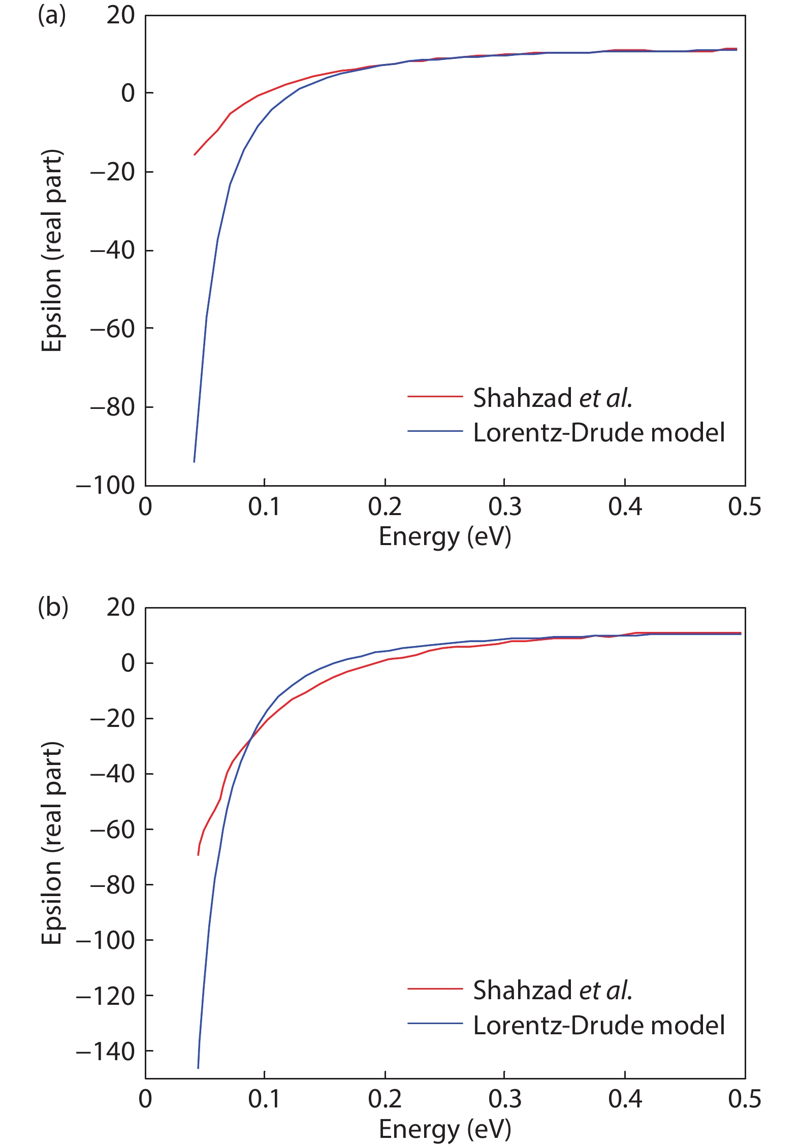
![]()
Figure 1.(Color online) Comparison between theoretical value and experimental value for carrier concentration of (a) 6 × 1019 cm–3 and (b) 1 × 1020 cm–3.
The percentages of error between the theoretically calculated value using the Lorentz-Drude model and the experimentally obtained value by Shahzad et al. at different wavelengths for p-silicon carrier concentration of 6 × 10¹⁹ and 1 × 1020 cm–3 has been shown in Tables 2 and 3, respectively.
From Fig. 1 and Table 2, it is observed that for a carrier concentration of 6 × 1019 cm–3, the percentage of error between the theoretical value and the experimental value is very high (>160%) for wavelengths greater than 9.69µm, high (40%) for wavelengths between 6.5 to 9.69 µm and very low (≤ 3.95%) for wavelengths less than 6.5 µm. For a carrier concentration of 1 × 1020 cm–3, the percentage of error is very high (>109.7%) for wavelengths greater than 26.23µm, high (20.35%–34.33%) for wavelengths between 3.86 to 17.69 µm and low (≤ 7.12%) for wavelengths smaller than 3.34 µm.
The Lorentz-Drude model mainly provides the frequency dependent dielectric permittivity of metals. In metals, electronic transition from the valence band to the conduction band takes place at a lower photon energy which is taken into consideration while theoretical modeling of any material is done using the Lorentz-Drude model. However, the band structure possessed by semiconductors like silicon is quite different compared to those of metals and the energy gap between the conduction band and valence band is also higher in semiconductors compared to metals. Thus, at lower photon energy, the dielectric property of doped silicon given by the Lorentz-Drude model, considering the contribution from interband transition of electrons, does not match with the experimental result as there is no interband transition practically. However, at higher photon energy, electrons in the semiconductor can absorb the required energy for interband transition just like metals. Thus, at higher photon energy, the Lorentz-Drude model can provide us with the more accurate values since the theoretical assumption regarding the interband transition also takes place practically. This difference in the theoretically predicted value and the experimentally obtained value at low photon energy has been depicted in Fig. 1. At higher photon energy, the theoretical and experimental value matches with each other as predicted by the theory. Analyzing the data from Tables 2 and 3, it is evident that the model shows a low percentage of error for wavelengths smaller than 3.34 µm. Thus, this model of heavily doped p-silicon can be used for the plasmonic devices, which work in the range of wavelengths smaller than 3.34 µm, which is the case for most of the plasmonic applications.
Heavily doped p-silicon can also be modeled at other carrier concentrations and wavelengths. The relationship of both the real part and imaginary part of the permittivity with carrier concentration and wavelength is almost linear. Fig. 2 shows the plot of relative permittivity against carrier concentration for different wavelengths.
![]()
Figure 2.(Color online) Relative permittivity (a) real part and (b) imaginary part versus carrier concentration at different wavelength.
3. Comparison with conventional plasmonic metals
Among the conventional plasmonic materials, gold and silver are the most commonly used metals. A number of models for gold and silver are already available for use. The complex dielectric permittivity of gold and silver has been determined using both the Drude model and Lorentz-Drude model considering the effect of both free electrons and bound-electrons in metals. The part on which free-electron effects act
and the part on which bound-electron effects act
where
Values of different parameters for obtaining the permittivity of gold and silver have been reported by Rakic et al.[
Since the relative permittivity is a complex quantity, it will have both real and imaginary parts. Fig. 3 shows the real part of both gold and silver plotted along with the real part of the permittivity of p-silicon for different carrier concentration.
![]()
Figure 3.(Color online) Real part of relative permittivity for silver, gold and, p-silicon for different values of carrier concentration of p-silicon.
From Fig. 3, it is observed that silver, gold and p-silicon, all have negative real parts of the permittivity after a certain wavelength. The real part of the complex permittivity for both gold and silver is larger than the p-silicon. This is mainly due to their high carrier concentration (≈1023 cm–3). The large real part of the permittivity causes polarization mismatch in many plasmonic devices when the interface is created with an insulator[
Comparison between the imaginary parts of the dielectric permittivity is shown in Fig. 4. The imaginary parts of the permittivity of both gold and silver are much larger than that of p-silicon even at a higher carrier concentration of p-silicon. Since the large value of the imaginary part is responsible for larger optical loss, plasmonic devices formed with p-silicon will suffer much lower optical loss than the conventional metal plasmonic devices.
![]()
Figure 4.(Color online) Imaginary part of relative permittivity for silver and gold, and p-silicon for different values of carrier concentration.
4. Waveguide formation and result analysis
A straight waveguide with a ring resonator is formed with a silicon–insulator–silicon structure instead of MIM. The waveguide is simulated and SPP propagation similar to the MIM waveguide is observed. For simulation purposes, commercial simulation software COMSOL Multiphysics was used. Fig. 5 shows the normalized electric field distribution at wavelength 1400 and 1800 nm respectively for the ring resonator structure formed with the silicon-air-silicon waveguide. From Fig. 5, it is clearly observable that SPPs are created and propagated along the interface of p-silicon and air. Thus, we can come to a conclusion that p-silicon can be used as a replacement of metal in plasmonic devices in order to support SPP propagation.
![]()
Figure 5.(Color online) Propagation of SPP along the silicon–air–silicon waveguide.
The comparison of the transmittance in a straight waveguide formed with silver-air-silver and gold-air-gold with the same structure formed with a silicon-air-silicon waveguide with different carrier concentration is shown in Fig. 6 which shows that, by doping the silicon up to a certain concentration, transmittance more than both the silver-air-silver and gold-air-gold can be achieved. The doped silicon waveguide can also be used to obtain transmission response of a notch filter similar to those of MIM waveguides by coupling the straight waveguide with a ring resonator as shown in Fig. 5. The notch type response of the ring resonator structure with MIM waveguides and doped silicon waveguide is shown in Fig. 7. The sensing characteristics of the ring resonator with doped silicon can be utilized to use it as a refractive index sensor by placing the sensing material in the ring waveguide. The resonant wavelength shifts with the change of refractive index, n, of the sensing material which is shown in Fig. 8. Similarly, in most of the plasmonic devices, the metals like gold and silver can be replaced by doped silicon of the required carrier concentration to enhance the performance of the devices and to provide a more suitable way of fabrication.
![]()
Figure 6.(Color online) Comparison of the transmittance between (a) the silver and p-silicon waveguide and (b) the gold and p-silicon waveguide.
![]()
Figure 7.(Color online) Notch type transmission response shown by ring resonators using gold, silver and psilicon.
![]()
Figure 8.(Color online) Sensing characteristics shown by ring resonators formed with heavily doped silicon.
5. Conclusion
A potential replacement of metals in plasmonic devices, heavily doped p-silicon is modeled here. The modeling parameters are found out for different carrier concentrations of p-silicon and the result is compared with the experimentally obtained result for the carrier concentration of 6 × 10¹⁹ and 1 × 1020 cm–3. In both cases, the error percentage for wavelengths smaller than 3.34 µm has been found to be ≤ 7.12% which trends to decrease gradually as the wavelength becomes smaller, since most of the plasmonic devices operate in the range of wavelengths smaller than 2 µm where the error percentage is expected to be much less than the error obtained here. Thus, the mathematical model can be considered as verified one for wavelengths smaller than 3.34 µm. The real part of the relative permittivity obtained in the model shows negative permittivity for a carrier concentration greater than 23 × 1020 cm–3. Thus, it will behave like metal after doping with a carrier concentration of than 23 × 1020 cm–3 and can be used in plasmonic devices instead of metal to guide SPPs, which is also observed here by simulation. Hence, we can come to a conclusion that heavily doped p-silicon can behave like metal and can be used as a replacement of metals in plasmonic devices which will help us to overcome optical loss, unbalanced polarization response and nanofabrication challenges possessed by metals.
References
[1] W L Barnes, A Dereux, T W Ebbesen. Surface plasmon subwavelength optics. Nature, 424, 824(2003).
[2] H Lu, X Liu, G Wang et al. Tunable high-channel-count bandpass plasmonic filters based on an analogue of electromagnetically induced transparency. Nanotechnology, 23, 444003(2012).
[3] H Q Wang, J B Yang, J J Zhang et al. Tunable band-stop plasmonic waveguide filter with symmetrical multiple-teeth-shaped structure. Opt Lett, 41, 1233(2016).
[4] P B Johnson, R W Christy. Optical constants of the noble metals. Phys Rev B, 6, 4370(1972).
[5] P R West, S Ishii, G V Naik et al. Searching for better plasmonic materials. Laser Photonics Rev, 4, 795(2010).
[6] W S Cai, U K Chettiar, A V Kildishev et al. Optical cloaking with metamaterials. Nat Photonics, 1, 224(2007).
[7]
[8]
[9] M Shahzad, G Medhi, R E Peale et al. Infrared surface plasmons on heavily doped silicon. J Appl Phys, 110, 123105(2011).
[10] D Linaschke, N Schilling, I Dani et al. Highly n-doped surfaces on n-type silicon wafers by laser-chemical processes. Energy Procedia, 55, 247(2014).
[11] I Mizushima, A Murakoshi, M Watanabe et al. Hole generation without annealing in high dose boron implanted silicon: Heavy doping by B12 icosahedron as a double acceptor. Jpn J Appl Phys, 33, 404(1994).
[12] L Viña, M Cardona. Effect of heavy doping on the optical properties and the band structure of silicon. Phys Rev B, 29, 6739(1984).
[13] Z Ma, Y Liu, L Deng et al. Heavily boron-doped silicon layer for the fabrication of nanoscale thermoelectric devices. Nanomaterials, 8, 77(2018).
[14] M Miyao, T Motooka, N Natsuaki et al. Change of the electron effective mass in extremely heavily doped n-type Si obtained by ion implantation and laser annealing. Solid State Commun, 37, 605(1981).
[15] G E Jellison, F A Modine, C W White et al. Optical properties of heavily doped silicon between 1.5 and 4.1 eV. Phys Rev Lett, 46, 1414(1981).
[16] et al. Precipitation, aggregation, and diffusion in heavily arsenic-doped silicon. Phys Rev B, 49, 2477(1994).
[17]
[18] M G Saber, N Abadía, D V Plant. CMOS compatible all-silicon TM pass polarizer based on highly doped silicon waveguide. Opt Express, 26, 20878(2018).
[19] Z P Qi, G H Hu, L Li et al. Design and analysis of a compact SOI-based aluminum/highly doped p-type silicon hybrid plasmonic modulator. IEEE Photonics J, 8, 1(2016).
[20] G V Naik, V M Shalaev, A Boltasseva. Alternative plasmonic materials: Beyond gold and silver. Adv Mater, 25, 3264(2013).
[21] Y B Chen, Z M Zhang. Heavily doped silicon complex gratings as wavelength-selective absorbing surfaces. J Phys D, 41, 095406(2008).
[22] D K Schroder, R N Thomas, J C Swartz. Free carrier absorption in silicon. IEEE J Solid-State Circuits, 13, 180(1978).
[23] M van Exter, D Grischkowsky. Carrier dynamics of electrons and holes in moderately doped silicon. Phys Rev B, 41, 12140(1990).
[24] A D Rakić, A B Djurišić, J M Elazar et al. Optical properties of metallic films for vertical-cavity optoelectronic devices. Appl Opt, 37, 5271(1998).
[25] A V Kildishev, V M Shalaev. Engineering space for light via transformation optics. Opt Lett, 33, 43(2008).
[26] W S Cai, U K Chettiar, A V Kildishev et al. Designs for optical cloaking with high-order transformations. Opt Express, 16, 5444(2008).

Set citation alerts for the article
Please enter your email address
© Copyright 2018-2021 | Chinese Laser Press. All Rights Reserved 沪ICP备15018463号-20