
[in Chinese], [in Chinese], [in Chinese], [in Chinese], [in Chinese], [in Chinese]. Surface plasmon enhanced infrared photodetection[J]. Opto-Electronic Advances, 2019, 2(1): 180026
- Opto-Electronic Advances
- Vol. 2, Issue 1, 180026 (2019)
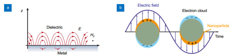
Fig. 1. (a ) Surface plasmon polariton at single interface. (b ) Localized surface plasma resonance for subwavelength metal nanoparticles. Figures reproduced from: (a) ref. 26, Nature Publishing Group; (b) ref. 27, Springer International Publishing AG.
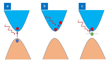
Fig. 2. Basic optical detection mechanism in semiconductors . (a ) Intrinsic absorption (interband transition), (b ) Free carrier absorption, (c ) Extrinsic absorption (impurity transition).
Fig. 3. Different plasmonic structures . (a ) Grating structure. (b ) Two-dimensional hole array structure. (c ) Nanorods inserted in absorber. (d ) Nanoparticle. (e ) Nanopyramids. (f ) Micropatch. Figures reproduced from: (a) ref. 28, Macmillan Publishers Limited; (b) ref. 31, AIP Publishing; (c) ref. 33, American Chemical Society; (d) ref. 34, Journal of Mechanical Engineering; (e) ref. 35, Optical Society of America.
Fig. 4. Plasmonic 2DSHA-hetero n-i-p photodetector . (a ) Schematic diagram of the device. (b ) Spectra of electric field enhancement in 2DSHA with a period of 900 nm at the hot spot position, as indicated in the inset. (c ) Room-temperature responsivity. (d ) Room-temperature blackbody detectivity. Figures reproduced from: ref. 30, AIP Publishing.
Fig. 5. Plasmonic 2DSHA-hetero n-InAsSb/n-GaSb photodetector . (a) Schematic diagram of the device. (b) Photocurrent spectral measured at room temperature. Figures reproduced from: (a) ref. 40, Springer Science+Business Media New York; (b) ref. 38.
Fig. 6. Schematic diagrams of plasmonic Schottky detectors. A gold patch on p-Si substrate with a gold grating on top . Figures reproduced from ref. 29, Optical Society of America.
Fig. 7. Schematic diagrams of plasmonic photoconductive detectors . (a ) Antenna assisted graphene detector. (b ) MSM plasmonic waveguide with Ge as absorber and Au as plasmonic cladding. Figures reproduced from: (a) ref. 46, American Chemical Society; (b) ref. 48, American Chemical Society.
Fig. 8. Schematic diagrams of plasmonic quantum type detectors . (a ) 2DSHA gold structure fabricated on the Ge/Si QDIP. (b ) Au nanoantenna embedded in the QD layer on SiO2 substrate. (c ) Plasmonic nano-disk arrays on QDIP. (d ) Plasmonic hole array patterned on top of the DWELL detector. Figures reproduced from: (a) ref. 31, AIP Publishing; (b) ref. 53, AIP Publishing; (c) ref. 54, The Royal Society of Chemistry; (d) ref. 56, Macmillan Publishers Limited.
Fig. 9. Schematic diagrams of plasmonic thermal detectors . (a ) A gold 2DSHA structure on top of ZnO pyroelectric layer. (b ) A unit cell of the plasmonic absorber consisting of symmetrical gold split cross resonator. Figures reproduced from: (a) ref. 59, American Chemical Society; (b) ref. 60, Optical Society of America.
Fig. 10. Schematic diagrams of plasmonic detectors . (a ) Scanning electron microscope (SEM) image of the detector integrated with plasmonic patch resonator array. (b ) SEM image of the CNT detector with plasmonic electrodes. Figure reproduced from: (a) ref. 61, Macmillan Publishers Limited; (b) ref. 62, American Chemical Society.

Set citation alerts for the article
Please enter your email address
© Copyright 2018-2021 | Chinese Laser Press. All Rights Reserved 沪ICP备15018463号-20