Infrared photodetectors have been used extensively in biomedicine, surveillance, communication and astronomy. However, state of the art technology based on III-V and II-VI compounds still lacks excellent performance for high-temperature operation. Surface plasmon polaritons (SPPs) have demonstrated their capability in improving the light detection from visible to infrared wave range due to their light confinement in subwavelength scale. Advanced fabrication techniques such as electron-beam lithography (EBL) and focused ion-beam (FIB), and commercially available numerical design tool like Finite-Difference Time-Domain (FDTD) have enabled rapid development of surface plasmon (SP) enhanced photodetectors. In this review article, the basic mechanisms behind the SP-enhanced photodetection, the different type of plasmonic nanostructures utilized for enhancement, and the reported SP-enhanced infrared photodetectors will be discussed.
Infrared photodetection has been widely used in both military and civilian purposes, including biomedicine, surveillance, communication and astronomy. Current detection technologies are mainly based on excellent optoelectronic absorbers such as indium gallium arsenide (InGaAs) in near infrared (NIR)1, mercury cadmium telluride (MCT) in middle infrared (MIR)2-3, and MCT and quantum well infrared (QWIP) structures in long infrared (LIR) ranges4. The photodetection relying on the absorption by sensitive optoelectronic materials has been inherently limited by the absorption law exp (-αd)5, where α is the absorption coefficient and d is thickness of the absorption layers. For sufficient photon absorption, the detection structure on one hand, requires high α, and on the other hand, requires large d to give high quantum efficiency. However, for an optimized absorber, α is fixed, therefore, very large d is required to ensure that. Nevertheless, the large reflection loss still limits the maximum quantum efficiency. Besides, the large value of d will bring some realistic difficulties, such as large stress and high cost of products in material growth and complex process in device manufacturing6.
The field of plasmonics studies the unique properties of light arising from the interaction between light with metallic nanostructures at sub-wavelength scale7-10. Those nanostructures own the capability of supporting collective electron excitations, known as surface plasmons. As surface plasmon resonance (SPR) occurs, the ability to concentrate light or produce large local field in extremely small volume enables the significant absorption of electromagnetic waves, therefore, facilitating the interaction between light and optoelectrical absorbers. This kind of property has been widely utilized for improving the quantum efficiency of solar cells11. At infrared range, metallic nanostructures are also integrated with semiconductor detectors to enhance the absorption of photons, therefore, to improve the photoelectrical conversion efficiency. Thanks to the state-of-the-art fabrication techniques such as electron-beam lithography (EBL) and focused ion-beam (FIB) milling, as well as commercially available numerical design tools like finite-difference time-domain (FDTD), the design and fabrication of metallic nanostructures for infrared range now become very effective. Metallic nanostructures with different configurations and metals can be used to integrate with traditional detection structures such as heterojunction structure12-17, Schottky diode18, quantum structures19, and thermal detector20. Combined with these structures, the photoresponse of those detectors can be significantly improved. These advances improve the performance of existing detection structures, and meanwhile they point out the direction of a new generation of infrared detection technologies.
The applications of surface plasmons in solar cell, biosensor, and manipulating light have been excellently reviewed21-22. This article will focus on the recent developments in surface plasmon enhanced infrared photodetection. The physics of surface plasmon and photodetection will be introduced first, followed by the plasmonic structures. Then, different kinds of plasmonic integrated photodetectors will be described. Possible further development will also be speculated.
Fundamentals
Surface plasmon
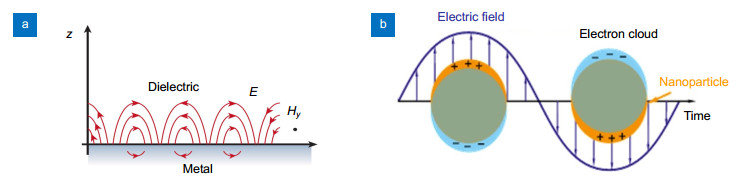
The quasi particle of light and collective electron oscillations along the metal-dielectric interface is referred to as surface plasmon polariton (SPP), which supports intense electromagnetic confinement in the deep subwavelength dimension21. The SPPs can be conventionally divided into two groups: propagating SPPs and localized SPPs. As shown in Fig. 1(a), single metal-dielectric interface can enable the excited SPPs to propagate for typically tens of micrometres along the interface. The solutions of Maxwell's equation require the momentum matching between the SPP and incident light for exciting the propagating SPPs, as shown in the following equation23:
where kSPP is the wavevector of the SPPs, k0 is the wavevector of light in free space, εm and εd are the permittivity of metal and dielectric, respectively. Eq. (1) requires an additional structure, like prism and corrugated-grating coupling structures, to be involved to assist in increasing the wavevector of light for satisfying the momentum matching22.
The excitation of localized SPPs (Fig. 1(b)) can be obtained by directly illuminating light on the curve surface of metal nanoparticles11. As localized SPR occurs, the optical electric field within (Ein) and out of (Eout) the subwavelength particle can be expressed as23:
where E0 is the static electric field, p is the electric dipole moment, r is the position vector of particle and ε0 is the permittivity in vacuum.
There is another unique property of surface plasmons that should be mentioned here as it has been widely studied for photoelectrical conversion, especially for solar cells. This method is based on the decay of surface plasmons, which can induce electron-hole pairs24 or nonequilibrium electrons25 in the metals or in semiconductors. The high energy electrons can contribute to photocurrent with appropriate architecture design.
Photodetection
The infrared photodetector is an important electronic device that converts infrared electromagnetic wave into electronic signal. We will first use a simple photodiode as an example to explain photodetection mechanism, which will later help to understand the contribution of plasmonic resonance. Photodetection can be achieved through various mechanisms illustrated in Fig. 2. The simplest mechanism is via the absorption of photon with higher energy than the semiconductor bandgap (Fig. 2(a)), which leads to the generation of electron-hole pairs in the absorption region. These electron hole pairs are then separated by a strong electric field and collected at their respective contacts5. In this way, a photocurrent is generated at the contacts. This kind of photodetection is based on intrinsic optical transition in optoelectronic semiconductors. As there are limited numbers of materials with bandgap energy in the infrared range, there have been various mechanisms proposed for infrared detection, including the use of free-carrier absorption (Fig. 2(b)) and impurity band absorption (Fig. 2(c)). In addition, based on different thermal sensitive mechanisms, thermal detectors can also respond well in infrared wave range.
The performance of a photodetector can be gauged by some figure of merits (FOM), namely the quantum efficiency, responsivity, noise equivalent power, and normalized detectivity. One of the most important FOM of photodetectors is the quantum efficiency (η), which is defined as the number of electron-hole pairs generated per incident photon (assuming the internal photoelectrical gain is unity), η=(1-r)(1-e-αd), where r is the reflectance, α is the absorption coefficient, and d is the absorption layer thickness. The other important FOM is the responsivity, R, which can be used to describe the photoelectric efficiency. It is defined as the output signal generated in detector in response to a unit incident power. Responsivity can also be described by the quantum efficiency as \begin{document}$ R = {I_p}/P = q\eta \lambda /hc $\end{document}(Ip is the photocurrent, P is the incident power on the detector, q is the unit charge element, η is the quantum efficiency, λ is the wavelength, h is the Planck constant, and c is the speed velocity in vacuum). For high photodetection performance, it is thus necessary to have high responsivity, which can be achieved by increasing the quantum efficiency, as indicated in the equation. The noise equivalent power (NEP) is the detectable power when the signal to noise ratio is equal to 1, which can be described as NEP=Ii/R (Ii is the noise current). The final FOM to evaluate the performance of a photodetector is the normalized Detectivity D*, which can be written in terms of NEP as D*=Ad(Δf)1/2/NEP, where, Ad is the detector area and Δf is the bandwidth5.
Surface plasmon enhanced photodetection
For an ideal photodiode, there exists a trade-off between quantum efficiency and thickness of absorption layer. According to the definition of quantum efficiency, higher quantum efficiency is achieved in a thicker absorption layer, but at the expense of longer transit time and thus slower response, as well as the cost of product in material growth. Therefore, optimizing the detector itself can no longer solve this problem and one needs to find other ways beyond the limitation of detector itself to increase the absorption coefficient in thin absorption layer, which can reduce the physical thickness of the absorption layer but maintain the optical thickness constant. Integrating a plasmonic structure with a detector is one of the popular strategies for realizing this objective, since at the metal-dielectric interface, the optical field can be enhanced by SPR. The interaction between SPP fields and absorption area results in trapping and concentrating light in subwavelength dimension, which can increase absorption inside detector, especially at the resonance frequency, and therefore enhance the photoresponse without sacrificing the physical thickness.
Plasmonic structures
In the infrared spectral region, the plasmonic structures of various geometrical shapes have been fabricated and integrated with the detectors, facilitating further in-depth exploration of plasmonic effect on photodetection performance. Due to the advanced fabrication techniques, like EBL which provides high resolution for features down to sub-10 nm, and FIB milling which can process the existing planar film26, as well as the commercially available designing software packages like FDTD and Comsol, the design and fabrication of metallic nanostructures for infrared range become very effective. One of the popular structures is plasmonic grating28 whose resonant modes are excited through phase matching between incident light and SPPs. As this structure is easily fabricated and integrated just by depositing the grating metal on top of detector29, it has been adopted in various detector types which will be discussed later. The plasmonic gratings have strong polarization-dependence on the incident electromagnetic waves, which is suitable for polarization-resolved photodetection. By changing the period of the grating, the resonant wavelength can be tuned. The other popular structure is two-dimensional metallic hole array structure which can achieve the extraordinary optical transmission (EOT) at resonant frequency30-32, thereby increasing the absorption efficiency in detector. For the normal incident light and square lattice array, the resonant wavelength can be deduced by the following equation:
where (i, j) are mode orders in x- and y- directions, a0 is the lattice constant for the hole array structure. According to this equation, one can roughly determine the geometrical dimension of the structures for specific wavelength. However, with consideration of the practical fabrication by EBL and FIB, these structures are usually designed for relatively longer IR range with typical size larger than that in visible range. The complementary structure of the hole array is the plasmonic metal cube array structure (Fig. 3(f)) (its resonance depends mainly on the metallic cube). The hole array and its complementary structure have been intensively studied on enhanced photodetection owing to their simplicity. Usually, for these structures, the duty cycle is chosen to be 50% to allow the largest enhanced absorption. In addition, the thickness of metals should be larger than the penetration depth of incident IR radiations to avoid disturbance of direct IR absorption. An order of magnitude performance enhancement can be expected with plasmonic hole arrays, providing that the generated photocarriers can be collected efficiently. There are other plasmonic structures based on the field enhancement associated with the localized SPR, such as nanorod33, nanoparticle34, nanopyramid35, and micropatch36, as shown in Fig. 3. The typical size of the particles should be much smaller than the detected wavelength to form subwavelength configuration. And they usually allow broadband enhancement compared to those plasmonic structures with propagated SPPs. These kinds of structures are widely used in improving the quantum efficiency of solar cells. They sometimes only require very simple spin-coating solution rather than relatively complicated EBL or FIB fabrication. These plasmonic particles typically operate in the visible range. Examples of different types of infrared photodetector integrated with different plasmonic structures to enhance the photodetection performance will be discussed in the following sections.
Figure 3.Different plasmonic structures. (a) Grating structure. (b) Two-dimensional hole array structure. (c) Nanorods inserted in absorber. (d) Nanoparticle. (e) Nanopyramids. (f) Micropatch. Figures reproduced from: (a) ref. 28, Macmillan Publishers Limited; (b) ref. 31, AIP Publishing; (c) ref. 33, American Chemical Society; (d) ref. 34, Journal of Mechanical Engineering; (e) ref. 35, Optical Society of America.
Recently group Ⅲ-Ⅴ materials have shown great potential for MIR detection, especially the InAsSb-based material for its better bandgap tunability and uniformity in material growth relative to the dominant MCT material. To further reduce the dark current and increase the operating temperature, InAsSb based heterostructure photodetectors have attracted much attention. However, due to the low absorption efficiency in MWIR range, increasing responsivity without sacrificing the device speed becomes an important issue to be solved. One popular approach is to integrate the plasmonic structure with the hetero device. An InAsSb-based hetero-n-i-p photodiode integrated with a two-dimensional square-lattice hole array (2DSHA) structure has been proposed, as sketched in Fig. 4(a)30. From patterning 2DSHA structure on top of device by using EBL, metal evaporation and lift-off process, the incident light can be strongly confined near the metal-dielectric interface. In order to position the fundamental resonance around the peak spectral response of the hetero-n-i-p photodiode (3.5 μm), the authors designed the 2DSHA plasmonic structure with period of 900 nm as derived in the equation (4), and the hetero photodiode with an active region of ~1 μm which is the same as the SPP penetration depth (δd) as obtained from the following equation,
Figure 4.Plasmonic 2DSHA-hetero n-i-p photodetector. (a) Schematic diagram of the device. (b) Spectra of electric field enhancement in 2DSHA with a period of 900 nm at the hot spot position, as indicated in the inset. (c) Room-temperature responsivity. (d) Room-temperature blackbody detectivity. Figures reproduced from: ref. 30, AIP Publishing.
where εm' and εd are the real permittivity of the gold and hetero device, respectively. As shown in Fig. 4(b), the numerically calculated electric field enhancement (|Ex, int/Ex, in|2) at the hot spot position indicates that the 2DSHA plasmonic effect can indeed contribute to the significant increase of field intensity for fundamental mode as well as other higher order modes. The clear increase in the measured room-temperature responsivity and detectivity (Figs. 4(c)-4(d)) for the 2DSHA-hetero detector also confirms the strong plasmonic effect. A room-temperature detectivities of 8 × 10⁹ Jones at 3.4 μm is demonstrated. In addition, it is observed that the improvement of performance can be controlled by modulating the overlap region between the depletion layer and SPP penetration depth. In practice, this can be achieved by tuning the depletion layer width (W) of the active region via adjusting the applied voltage bias (V), i.e., W ∝ (Vbi-V)1/2. In this manner, the 380% tuning depth (enhanced percentage) over 0.32 V bias change (from -0.15 to 0.17 V) could be realized37.
Except for the plasmon-enhanced single-band detection, a plasmonic structure enhanced dual-band detector can be realized by integrating the 2DSHA with a n-InAsSb/n-GaSb hetero-detector (Fig. 5(a))38. Through matching the resonant modes of the 2DSHA with InAsSb and GaSb absorption bands, it is found that the room-temperature photocurrent spectral demonstrates obvious enhancement in two separate bands which are 3.4 μm (MIR) for InAsSb and 1.7 μm (NIR) for GaSb, respectively, as shown in Fig. 5(b). The highest room-temperature detectivities of 1.4×10⁹ Jones at 3.4 μm and 1.5×10¹¹ Jones at 1.7 μm were achieved, which are comparable with state-of-the-art MIR and NIR photodetectors for single-band detection. The other work39 also studied this dual-color plasmonic enhancement and found that at a forward applied bias, the plasmonic detector can achieve the dual-band detection with highest responsivity. Several studies have also been carried out on explaining the plasmonic effect for the n-InAsSb/n-GaSb hetero-detector40, 41. In addition to the hetero n-i-p photodiode, the plasmonic structure has been integrated with the nBn barrier structure42, 43. The quantum efficiency was increased to 57% via the 2D plasmonic grating patterned on top of device.
Figure 5.Plasmonic 2DSHA-hetero n-InAsSb/n-GaSb photodetector. (a) Schematic diagram of the device. (b) Photocurrent spectral measured at room temperature. Figures reproduced from: (a) ref. 40, Springer Science+Business Media New York; (b) ref. 38.
A Schottky type photodetector can be used to detect radiation below the bandgap energy of the semiconductor via internal photoemission (IPE). Figure 3(a) shows the sketch of a grating-assisted Schottky photodetector28. It consists of an Au grating layer on an n-doped silicon substrate, with a very thin titanium layer in between to determine the height of Schottky barrier and adhere the grating layer to the silicon substrate. With the plasmonic grating configuration44, this Schottky detector combines narrow spectral response at resonant wavelength with the hot electron-assisted photodetection. Compared to the previous antenna-based Schottky photodetector, a significant increase in its responsivity and internal quantum efficiency (IQE) is observed. Alavirad et al. 29 further designed a broadband silicon plasmonic Schottky photodetector with an Au grating on top of a thin Au patch, defined by EBL and optical lithography, respectively, as sketched in Fig. 6. They observed strong responsivity enhancement in the sub-bandgap regime by exciting the SPPs at the gold-silicon interface. Another type of broadband plasmonic Schottky detector35 is shown in Fig. 3(e), where Al was patterned on the apex of pyramid-shaped silicon wafer. The designed pyramidally shaped plasmonic concentrators are used to get high responsivity, as the light can be collected from the large cross-section of pyramid and converge on the peak region where it is absorbed and creates hot electrons with sufficiently high energy to overcome the Schottky barrier. Such a detector can achieve the nanoscale confinement together with large collection efficiency. These detectors have important advantages such as speed, simplicity, compatibility with silicon, and low-cost fabrication.
Figure 6.Schematic diagrams of plasmonic Schottky detectors. A gold patch on p-Si substrate with a gold grating on top. Figures reproduced from ref. 29, Optical Society of America.
The photoconductive type detector operates for the photons with energy hν larger than the bandgap energy Eg, which change the semiconductor electrical conductivity by exciting electron-hole pairs5. It is well known that graphene material is a good choice for photoconductor because of its fast and broadband response. However, it is difficult for graphene photoconductor to achieve high responsivity due to its short photocarrier lifetime and low absorption efficiency. One promising approach is to utilize the plasmonic structures36, 45. An end-to-end plasmonic antenna structure was fabricated on a graphene sheet, as shown in Fig. 7(a)46. With assistance of the plasmonic nanoantenna, the electric field intensity is strongly enhanced inside the nanoantenna gaps47, concentrating the light within the gap region for realizing high responsivity in MIR photodetection. In terms of the traditional MCT photoconductive detector, Jaksic et al.34 applied transparent conductive oxide (TCO) plasmonic nanoparticles on top of the MCT detector (Fig. 3(d)) to directly increase light absorption inside active region through the local electric field enhancement, via the existence of evanescent plasmon modes. In this manner, the MCT photoconductor obtains a significant increase in responsivity in the MIR range. Germanium photoconductive detector with a plasmonic structure has also been explored by Salamin et al. It consists of a metal-semiconductor-metal (MSM) waveguide with Ge as the active region in the plasmonic gold antenna48, as shown in Fig. 7(b). The light absorption inside the active region is increased via the SPPs generated by the evanescently coupled photons.
Figure 7.Schematic diagrams of plasmonic photoconductive detectors. (a) Antenna assisted graphene detector. (b) MSM plasmonic waveguide with Ge as absorber and Au as plasmonic cladding. Figures reproduced from: (a) ref. 46, American Chemical Society; (b) ref. 48, American Chemical Society.
As the epitaxial growth technique develops, the device structure can be engineered to low dimension, such as quantum well (QW) structure, where the carrier is confined in a narrow enough region so that the device performance improvements can be expected. However, similar to the graphene photoconductor, the major obstacle for low-dimensional MIR detectors is the low light absorption inside the absorber layer due to the limited thickness of active region. One solution is to incorporate the plasmonic structure inside absorber layer or in other places. It has been reported that integrating a periodic hole array structure patterned in the gold film with the InGaAs/InP QWIP can convert the normal-incident photons into SPPs, which in turn excites the carrier intersubband transition in the QWIP, leading to an enhancement in the detector spectral response and detectivity in the MIR region19.
In recent years, quantum dot infrared photodetectors (QDIP) have demonstrated great potential for MIR detection mainly due to their carrier confinement in all directions, in contrast to QWIP which can only confine carriers in one dimension. One of the popular plasmonic structures for enhancing QDIP response is the periodic hole array structure, where the metal film was patterned on the front- or back-side of QDIP detector. Here, we take the Ge/Si QDIP shown in Fig. 8(a)31 as an example. The 2DSHA EOT effect for exciting the SPPs at the interface of metal hole array and dielectric layer significantly enhances the QDIP quantum efficiency and responsivity49-52. In addition to the 2DSHA structure, there are also reports on plasmonic dipole arrays in an MCT QD layer53 (Fig. 8(b)) and the gold nanodisk arrays in the HgSe QD film (Fig. 8(c))54 for enhancement in MIR range.
Figure 8.Schematic diagrams of plasmonic quantum type detectors. (a) 2DSHA gold structure fabricated on the Ge/Si QDIP. (b) Au nanoantenna embedded in the QD layer on SiO2 substrate. (c) Plasmonic nano-disk arrays on QDIP. (d) Plasmonic hole array patterned on top of the DWELL detector. Figures reproduced from: (a) ref. 31, AIP Publishing; (b) ref. 53, AIP Publishing; (c) ref. 54, The Royal Society of Chemistry; (d) ref. 56, Macmillan Publishers Limited.
Except for the QDIP structure, quantum dots-in-a-well (DWELL) architecture was proposed by Liu et al., in which the quantum dots are located inside the quantum well layer55. The DWELL detector combines the advantages of quantum well and quantum dots, such as easy control of operating wavelength range for quantum well structure, and low dark current for quantum dot structure. Lee et al.56 improved this detector by incorporating a 2DSHA plasmonic structure on the top of the InAs/InGaAs DWELL structure, as sketched in Fig. 8(d). They observed a ~160% increase in the voltage signal to noise ratio at the resonant wavelength. Besides, the quantum cascade detectors (QCD) are also very promising for large-scale FPA57. It is found that a 2DSHA fabricated on top of the detector active region could also increase the light absorption in QCD via the same plasmonic EOT effect58.
Thermal type
Figure 9(a) shows a thermal detector consisting of a plasmonic perfect absorber on a pyroelectric ZnO layer, which was fabricated by colloidal-mask lithography and reactive-ion etching59. The metamaterial absorber leads to a strong optical field and high thermal concentration in pyroelectric detector. By tuning the resonance wavelength of the plasmonic 2DSHA, excellent spectrally selective absorptivity at plasmonic resonances and significantly enhanced responsivity can be achieved. Apart from the 2DSHA structure, a new architecture whose unit cell is a symmetrical split cross resonator (Fig. 9(b)) is proposed, and a narrowband and high absorption in LIR was demonstrated60.
Figure 9.Schematic diagrams of plasmonic thermal detectors. (a) A gold 2DSHA structure on top of ZnO pyroelectric layer. (b) A unit cell of the plasmonic absorber consisting of symmetrical gold split cross resonator. Figures reproduced from: (a) ref. 59, American Chemical Society; (b) ref. 60, Optical Society of America.
There are also reports on other types of detectors which show enhanced detection performance. One example is the LIR quantum-well photodetector which consists of plasmonic sub-wavelength metallic resonators, where the square metallic patches cover the absorber and are connected via leads as sketched in Fig. 10(a). The enhancement in responsivity occurs because the plasmonic resonators increase the local field-intensity in absorption layer, and the plasmonic antenna extends the photon collection area without increasing the electrical area61. In another example, Huang et al. introduced periodic axe-like plasmonic electrodes to the carbon nanotube (CNT) detector (Fig. 10(b)). In this device, the photogenerated carriers can be collected more effectively and light absorption inside the detector can be significantly increased62.
Figure 10.Schematic diagrams of plasmonic detectors. (a) Scanning electron microscope (SEM) image of the detector integrated with plasmonic patch resonator array. (b) SEM image of the CNT detector with plasmonic electrodes. Figure reproduced from: (a) ref. 61, Macmillan Publishers Limited; (b) ref. 62, American Chemical Society.
Surface plasmons for enhancing infrared detection have been widely investigated due to their capability of confining electromagnetic waves within the metal-absorber interfaces, and exciting achievements of SP-enhanced photodetectors already demonstrated. As most MIR and LIR photodetectors works at low temperature, the demonstrated progress of SP-enhanced photodetections bring a step closer towards infrared photodetectors operating at higher temperature. From the application perspective, both detection performance and fabrication cost remain the important issues to be considered. Most of the SP-enhanced photodetectors presented here employ expensive gold as the metal due to its stability and chemical inertness. This has motivated the exploration of non-noble metals for plasmonic applications. Germanium and aluminum have been shown as promising candidates for plasmonics and photodetection enhancement35, 42, 63.
Multicolor photodetection is regarded as the next generation infrared photodetection. This is where plasmonic structures provides multicolor enhancement through their multi-resonance modes, which is achieved through matching the multiple resonance modes from a single plasmonic structure with different absorption bands. The challenge faced for the multicolor photodetectors is the availability of the semiconductors that should be lattice-matched to ensure good quality of materials. Thus, optimized growth techniques and methods are expected to exploit to realize multicolor semiconductor absorbers.
In addition to the applications in a single element form, infrared photodetectors are widely utilized as focal plane arrays. As most SP-enhanced photodetection works focus on single element photodetection, further developments of SP-enhanced detection into large linear or planar arrays are expected. For this, one can try to fabricate the plasmonic unit cell arrays on the backside of the normal focal planar arrays with flip-chip method to the read-out circuit. This requires a very careful and complicated fabrication of metallic structures on the very thin substrate and the whole arrays. Even though the fabrication of large area of plasmonic metallic structures by EBL is time-consuming especially in the NIR and MIR range, where nanoscale subwavelength metallic structures are usually required to form those plasmonic structures. In LIR, normal photolithography techniques may be possible for fabricating subwavelength structures with microscale size. Thus, modified EBL fabrication technology may also be required. Of course, the industrial high-precision photolithograph can reach sub-micro size, but it is very expensive and usually only suitable for Si-based CMOS rather for Ⅲ-Ⅴ or Ⅱ-Ⅴ based infrared optoelectrical materials. With the enhanced detectivity of the photodetectors associated with the plasmonic structures, the imaging systems with focal plane arrays are expected to show better performance and operate at higher temperatures.
Besides, with the progress of fabrication technologies, metallic structures with much smaller characteristic size or much complicated 3D geometry may be achievable. This will further increase the light confinement within the absorber, resulting in further improved detection performance.
Acknowledgements
This work is supported by A*STAR (Grant No. 1720700038 and SERC A1883c0002), the Ministry of Education (RG177/17), Singapore; and Asian Office of Aerospace Research and Development (FA2386-17-1-0039).
Author contributions
J C Tong and F Suo drafted manuscript with equal contribution. D H Zhang supervised the work and finalized manuscript with inputs of all authors.
Competing interests
The authors declare no competing financial interests.