Journals >Opto-Electronic Advances
Contents


2019
Volume: 2 Issue 1
3 Article(s)
Export citation format
Contents

[in Chinese]
[in Chinese]
Opto-Electronic Advances
- Publication Date: Jan. 01, 1900
- Vol. 2, Issue 1, 1 (2019)


Review
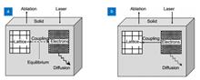
Laser machining of transparent brittle materials: from machining strategies to applications
[in Chinese], [in Chinese], [in Chinese], [in Chinese], and [in Chinese]
Transparent brittle materials such as glass and sapphire are widely concerned and applied in consumer electronics, optoelectronic devices, etc. due to their excellent physical and chemical stability and good transparency. Growing research attention has been paid to developing novel methods for high-precision and high-qTransparent brittle materials such as glass and sapphire are widely concerned and applied in consumer electronics, optoelectronic devices, etc. due to their excellent physical and chemical stability and good transparency. Growing research attention has been paid to developing novel methods for high-precision and high-quality machining of transparent brittle materials in the past few decades. Among the various techniques, laser machining has been proved to be an effective and flexible way to process all kinds of transparent brittle materials. In this review, a series of laser machining methods, e.g. laser full cutting, laser scribing, laser stealth dicing, laser filament, laser induced backside dry etching (LIBDE), and laser induced backside wet etching (LIBWE) are summarized. Additionally, applications of these techniques in micromachining, drilling and cutting, and patterning are introduced in detail. Current challenges and future prospects in this field are also discussed..
Opto-Electronic Advances
- Publication Date: Jan. 01, 1900
- Vol. 2, Issue 1, 180017 (2019)
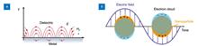
Surface plasmon enhanced infrared photodetection
[in Chinese], [in Chinese], [in Chinese], [in Chinese], [in Chinese], and [in Chinese]
Infrared photodetectors have been used extensively in biomedicine, surveillance, communication and astronomy. However, state of the art technology based on III-V and II-VI compounds still lacks excellent performance for high-temperature operation. Surface plasmon polaritons (SPPs) have demonstrated their capability in Infrared photodetectors have been used extensively in biomedicine, surveillance, communication and astronomy. However, state of the art technology based on III-V and II-VI compounds still lacks excellent performance for high-temperature operation. Surface plasmon polaritons (SPPs) have demonstrated their capability in improving the light detection from visible to infrared wave range due to their light confinement in subwavelength scale. Advanced fabrication techniques such as electron-beam lithography (EBL) and focused ion-beam (FIB), and commercially available numerical design tool like Finite-Difference Time-Domain (FDTD) have enabled rapid development of surface plasmon (SP) enhanced photodetectors. In this review article, the basic mechanisms behind the SP-enhanced photodetection, the different type of plasmonic nanostructures utilized for enhancement, and the reported SP-enhanced infrared photodetectors will be discussed..
Opto-Electronic Advances
- Publication Date: Jan. 01, 1900
- Vol. 2, Issue 1, 180026 (2019)

© Copyright 2018-2021 | Chinese Laser Press. All Rights Reserved 沪ICP备15018463号-20