
Qingqing Wang, Yun Zheng, Chonghao Zhai, Xudong Li, Qihuang Gong, Jianwei Wang. Chip-based quantum communications[J]. Journal of Semiconductors, 2021, 42(9): 091901
- Journal of Semiconductors
- Vol. 42, Issue 9, 091901 (2021)
Abstract
1. Introduction
The security of quantum communication (e.g., quantum key distribution; QKD) is enabled by the fundamental principles of quantum mechanics[
The first QKD protocol was proposed by Bennett and Brassard in 1984[
The state-of-the-art photonic quantum technologies have allowed the experimental realizations of thousands of kilometers ground-to-satellite QKDs[
2. Integrated QKD transceivers
The preparation-measurement quantum key distribution (PM-QKD) represents a major class of quantum communication protocols, such as differential phase shift (DPS) and coherent one way (COW) protocols. This type of protocol separates the communication system into two parts which are transmitter and receiver. The first realization of PM-QKD is mainly implemented with bulk-optic devices, for example from the seminal QKD experiments[
In 2004, a pioneering work by researchers in NTT reported the first integrated QKD devices in silica waveguide light-wave circuits, which demonstrated the encoding and decoding of quantum keys in integrated Mach-Zehnder interferometers[
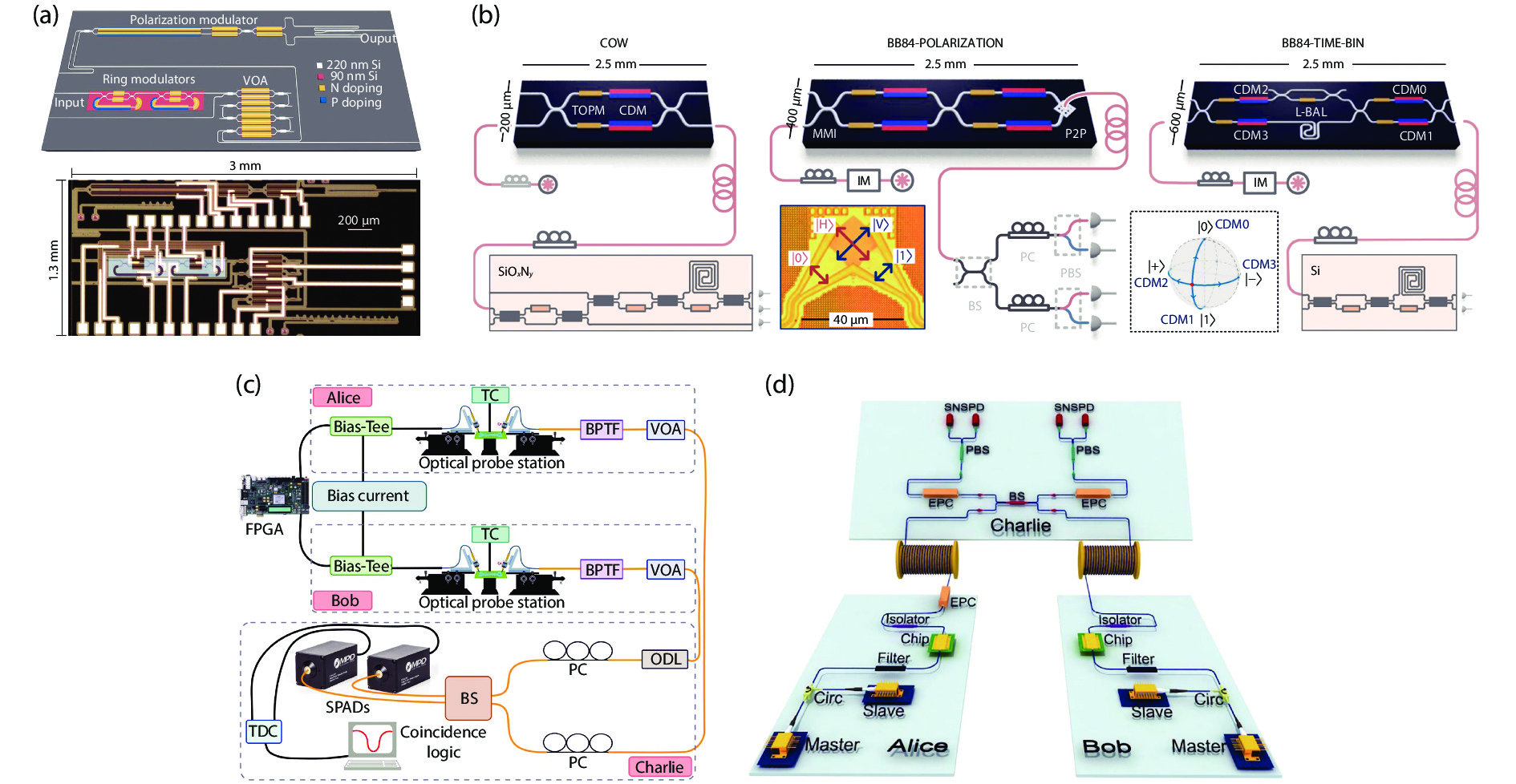
Several works have shown that silicon photonics are capable of implementing quantum communication tasks. For example, in Fig. 1(a) it shows a polarization-encoding QKD transmitter in a silicon chip[
![]()
Figure 1.(Color online) Integrated silicon photonic QKD transmitters. (a) Polarization-encoding PM-QKD transmitter, consisting of ring modulators, VOAs, and polarization modulators[
The QKD transmitter integrates ring modulators for light pulse generation, a variable optical attenuator (VOA) weakening power down to single-photon level, and a polarization modulator for the preparation of two orthogonal polarization bases. In 2017, researchers in Bristol reported a QKD transceiver that allows high-fidelity and high-speed quantum operations of single photon states, and also reaches estimated asymptotic secret key rates of up to 916 kbps and QBER as low as 1.01% in a 20 km fiber[
Quantum key information was carried in the polarization of single photons, which was implemented by two-dimensional grating coupler. Furthermore, recent demonstrations of chip-enabled metropolitan QKD system[
The III–V compound semiconductors such as InP enable light emissions and high-speed modulations of photons, thanks to their direct bandgap property[
![]()
Figure 2.(Color online) Integrated InP photonic QKD transmitters. (a) A chip-to-chip QKD system between a 2 × 6 mm2 InP transmitter and a 2 × 32 mm2 SiO
Despite the unconditional security in ideal QKD models, possible security-threatening attacks have appeared in real-world physical implementations. In particular, due to the complexity of detection systems and the inconsistency between theory and experiments, many attacks are aimed at detectors[
3. Integrated photonics for entanglement-based quantum communications
Entanglement plays a key role in quantum cryptography[
On-chip parametric sources and artificial atomic sources able to generate entangled-photon pairs have been reported in a range of material platforms. Artificial atomic structures such as quantum dots, defects, and dopants represent excellent quantum systems, which have allowed the generation of single photons, entangled photons, and spin-photon entanglement. Engineering the interactions of solid-state atoms and photons in nanostructures can significantly improve the entanglement quality. For example, entangled photon pair source with high brightness and indistinguishability was realized by embedding quantum dots in photonic nanostructures[
![]()
Figure 3.(Color online) On-chip entangled photon sources. (a) Generation of entangled photons from a single quantum dot embedding in photonic nanostructures[
Tight confinement of light in optical waveguides or structures enables enhancement of nonlinear optical effects (e.g., second-order and third-order nonliear effects), which allow the efficient generation of entangled photon-pairs via the spontaneous parametric down conversion (SPDC) or spontaneous four-wave mixing (SFWM) process, respectively. Typical on-chip parametric sources on the lithium niobate (LN), gallium arsenide (GaAs), Si and SixNy materials have been reported. Fig. 3(b) shows a thin-film periodically poled lithium niobate (PPLN) waveguide, which is able to generate energy-time entanglement at telecom wavelength with high brightness and coincidences-to-accidentals value[
The implementation of on-chip entanglement-based quantum communication protocols has become possible thanks to the capabilities of on-chip generations and manipulations of entangled photon pairs in different degrees-of-freedoms of photons[
Recent technological progress of integrated quantum photonic devices has allowed the implementation of quantum communication protocols beyond a single chip, which is key to future quantum networks[
![]()
Figure 4.(Color online) Chip-based entanglement distribution and quantum teleportation. (a) Silicon photonic circuit diagram for a chip-to-chip entanglement distribution experiment[
4. Recent development of on-chip quantum memories
Long distance distributions of entanglement and large-scale implementations of quantum network rely on quantum memories and quantum relays[
Note that other systems, such as vacancy centers in diamond, have proved to be great potential platforms[
To store the flying qubit state in the static qubit, an ideal method is to employ an absorbing matter that can absorb the photon with high probability and re-emit an identical photon some time later. In this way, the information carried by the photon is preserved in the matter in a fully controllable way. The rare-earth ions doped crystal (REIC) is one of the most promising solid-state quantum memory systems, featuring a broad inhomogeneous absorption spectrum up to GHz and a long coherence time up to millisecond at cryogenic temperatures[
where
Significant effort has been put into the experimental realizations of REIC quantum memory, both in bulk materials[
![]()
Figure 5.(Color online) Integrated quantum memories in the ERIC system. (a) An optical microscope image of five quantum memories in laser-written optical waveguides[
In general, the REIC quantum memory offers nearly optimal fidelity and on-demand storage time. However, the efficiency of most reported experiments is below 30%, and the efficiency of the forward collecting scheme in to-date experiments is up bounded by 54.1%[
5. Discussion and conclusion
The development of chip-based QKD devices and systems is still in its infancy, which mainly focuses on the proof-of-principle demonstrations of standard QKD protocols. One significant effort is to monolithically integrate key quantum optical components in a semiconductor chip for the purpose of key distribution and information sharing between integrated photonic chips. The relative high excess loss of integrated photonics makes it challenging to realize fully device-independent QKD systems.
The state-of-the-art bulk-optics QKD systems enable satellite-relayed global-scale quantum communication networks[
Integrated quantum photonics has become an important platform for the development of quantum information processing and quantum communication. Many leading candidates have emerged, such as indium phosphide, silicon, silicon nitride and lithium niobate. In the future, it can be expected to deliver chip-based QKD transmitters and receivers with miniature size, low cost, high stability and flexible portability. Broadly speaking, large-scale integrations and reliable operations of integrated quantum photonic devices and circuits will ultimately benefit the formation of powerful quantum information processing nodes for the future quantum internet.
Acknowledgements
We acknowledge support from the Natural Science Foundation of China (61975001), National Key R&D Program of China (2018YFB1107205), Beijing Natural Science Foundation (Z190005), and the Key R&D Program of Guangdong Province (2018B030329001).
References
[1] N Gisin, R Thew. Quantum communication. Nat Photonics, 1, 165(2007).
[2] W K Wootters, W H Zurek. A single quantum cannot be cloned. Nature, 299, 802(1982).
[3] C H Bennett, G Brassard. Quantum cryptography: Public key distribution and coin tossing. Theor Comput Sci, 560, 7(2014).
[4] P W Shor, J Preskill. Simple proof of security of the BB84 quantum key distribution protocol. Phys Rev Lett, 85, 441(2000).
[5] . Quantum cryptography based on Bell's theorem. Phys Rev Lett, 67, 661(1991).
[6] M Curty, M Lewenstein, N Lütkenhaus. Entanglement as a precondition for secure quantum key distribution. Phys Rev Lett, 92, 217903(2004).
[7] S K Liao, W Q Cai, W Y Liu et al. Satellite-to-ground quantum key distribution. Nature, 549, 43(2017).
[8] C H Bennett, F Bessette, G Brassard et al. Experimental quantum cryptography. J Cryptol, 5, 3(1992).
[9] Y A Chen, Q Zhang, T Y Chen et al. An integrated space-to-ground quantum communication network over 4, 600 kilometres. Nature, 589, 214(2021).
[10] T Honjo, K Inoue, H Takahashi. Differential-phase-shift quantum key distribution experiment with a planar light-wave circuit Mach-Zehnder interferometer. Opt Lett, 29, 2797(2004).
[11] P Sibson, J E Kennard, S Stanisic et al. Integrated silicon photonics for high-speed quantum key distribution. Optica, 4, 172(2017).
[12] C X Ma, W D Sacher, Z Y Tang et al. Silicon photonic transmitter for polarization-encoded quantum key distribution. Optica, 3, 1274(2016).
[13] D Bunandar, A Lentine, C Lee et al. Metropolitan quantum key distribution with silicon photonics. Phys Rev X, 8, 021009(2018).
[14] M Avesani, L Calderaro, M Schiavon et al. Full daylight quantum-key-distribution at 1550 nm enabled by integrated silicon photonics. npj Quantum Inf, 7, 93(2021).
[15] A Orieux, E Diamanti. Recent advances on integrated quantum communications. J Opt, 18, 083002(2016).
[16] P Sibson, C Erven, M Godfrey et al. Chip-based quantum key distribution. Nat Commun, 8, 1(2017).
[17] L Lydersen, C Wiechers, C Wittmann et al. Hacking commercial quantum cryptography systems by tailored bright illumination. Nat Photonics, 4, 686(2010).
[18] Y Zhao, C H F Fung, B Qi et al. Quantum hacking: Experimental demonstration of time-shift attack against practical quantum-key-distribution systems. Phys Rev A, 78, 042333(2008).
[19] V Makarov, A Anisimov, J Skaar. Effects of detector efficiency mismatch on security of quantum cryptosystems. Phys Rev A, 74, 022313(2006).
[20] H K Lo, M Curty, B Qi. Measurement-device-independent quantum key distribution. Phys Rev Lett, 108, 130503(2012).
[21] C K Hong, Z Y Ou, L Mandel. Measurement of subpicosecond time intervals between two photons by interference. Phys Rev Lett, 59, 2044(1987).
[22] C Agnesi, B da Lio, D Cozzolino et al. Hong–Ou–Mandel interference between independent III–V on silicon waveguide integrated lasers. Opt Lett, 44, 271(2019).
[23] J G Rarity, P R Tapster, R Loudon. Non-classical interference between independent sources. J Opt B, 7, S171(2005).
[24] K J Wei, W Li, H Tan et al. High-speed measurement-device-independent quantum key distribution with integrated silicon photonics. Phys Rev X, 10, 031030(2020).
[25] H Semenenko, P Sibson, M G Thompson et al. Interference between independent photonic integrated devices for quantum key distribution. Opt Lett, 44, 275(2019).
[26] H Semenenko, P Sibson, A Hart et al. Chip-based measurement-device-independent quantum key distribution. Optica, 7, 238(2020).
[27] S Wehner, D Elkouss, R Hanson. Quantum Internet: A vision for the road ahead. Science, 362, eaam9288(2018).
[28] J F Clauser, M A Horne, A Shimony et al. Proposed experiment to test local hidden-variable theories. Phys Rev Lett, 23, 880(1969).
[29] A Acín, S Massar, S Pironio. Efficient quantum key distribution secure against no-signalling eavesdroppers. New J Phys, 8, 126(2006).
[30] A Acín, N Brunner, N Gisin et al. Device-independent security of quantum cryptography against collective attacks. Phys Rev Lett, 98, 230501(2007).
[31] M McKague. Device independent quantum key distribution secure against coherent attacks with memoryless measurement devices. New J Phys, 11, 103037(2009).
[32] U Vazirani, T Vidick. Fully device-independent quantum key distribution. Phys Rev Lett, 113, 140501(2014).
[33] J Yin, Y Cao, Y H Li et al. Satellite-based entanglement distribution over 1200 kilometers. Science, 356, 1140(2017).
[34] J Liu, R B Su, Y M Wei et al. A solid-state source of strongly entangled photon pairs with high brightness and indistinguishability. Nat Nanotechnol, 14, 586(2019).
[35] J Zhao, C X Ma, M Rüsing et al. High quality entangled photon pair generation in periodically poled thin-film lithium niobate waveguides. Phys Rev Lett, 124, 163603(2020).
[36] J C Duan, J N Zhang, Y J Zhu et al. Generation of narrowband counterpropagating polarization-entangled photon pairs based on thin-film lithium niobate on insulator. J Opt Soc Am B, 37, 2139(2020).
[37] C Autebert, N Bruno, A Martin et al. Integrated AlGaAs source of highly indistinguishable and energy-time entangled photons. Optica, 3, 143(2016).
[38] J W Wang, S Paesani, Y H Ding et al. Multidimensional quantum entanglement with large-scale integrated optics. Science, 360, 285(2018).
[39] G Corrielli, A Crespi, R Geremia et al. Rotated waveplates in integrated waveguide optics. Nat Commun, 5, 4249(2014).
[40] X Zhang, B A Bell, A Mahendra et al. Integrated silicon nitride time-bin entanglement circuits. Opt Lett, 43, 3469(2018).
[41] C L Li, D J Liu, D X Dai. Multimode silicon photonics. Nanophotonics, 8, 227(2018).
[42] L T Feng, M Zhang, X Xiong et al. On-chip transverse-mode entangled photon pair source. npj Quantum Inf, 5, 2(2019).
[43] J W Silverstone, D Bonneau, K Ohira et al. On-chip quantum interference between silicon photon-pair sources. Nat Photonics, 8, 104(2014).
[44] J W Silverstone, R Santagati, D Bonneau et al. Qubit entanglement between ring-resonator photon-pair sources on a silicon chip. Nat Commun, 6, 7948(2015).
[45] D Grassani, S Azzini, M Liscidini et al. Micrometer-scale integrated silicon source of time-energy entangled photons. Optica, 2, 88(2015).
[46] F Mazeas, M Traetta, M Bentivegna et al. High-quality photonic entanglement for wavelength-multiplexed quantum communication based on a silicon chip. Opt Express, 24, 28731(2016).
[47] S Paesani, M Borghi, S Signorini et al. Near-ideal spontaneous photon sources in silicon quantum photonics. Nat Commun, 11, 2505(2020).
[48] J Suo, S Dong, W Zhang et al. Generation of hyper-entanglement on polarization and energy-time based on a silicon micro-ring cavity. Opt Express, 23, 3985(2015).
[49] F X Wang, W Q Wang, R Niu et al. Quantum key distribution with on-chip dissipative kerr soliton. Laser Photonics Rev, 14, 1900190(2020).
[50] J W Wang, F Sciarrino, A Laing et al. Integrated photonic quantum technologies. Nat Photonics, 14, 273(2020).
[51] J W Wang, D Bonneau, M Villa et al. Chip-to-chip quantum photonic interconnect by path-polarization interconversion. Optica, 3, 407(2016).
[52] J G Ren, P Xu, H L Yong et al. Ground-to-satellite quantum teleportation. Nature, 549, 70(2017).
[53] D Gottesman, I L Chuang. Demonstrating the viability of universal quantum computation using teleportation and single-qubit operations. Nature, 402, 390(1999).
[54] B J Metcalf, J B Spring, P C Humphreys et al. Quantum teleportation on a photonic chip. Nat Photonics, 8, 770(2014).
[55] X Y Lu, Q Li, D A Westly et al. Chip-integrated visible–telecom entangled photon pair source for quantum communication. Nat Phys, 15, 373(2019).
[56] M V G Dutt, L Childress, L Jiang et al. Quantum register based on individual electronic and nuclear spin qubits in diamond. Science, 316, 1312(2007).
[57] T Gaebel, M Domhan, I Popa et al. Room-temperature coherent coupling of single spins in diamond. Nat Phys, 2, 408(2006).
[58] R Hanson, F M Mendoza, R J Epstein et al. Polarization and readout of coupled single spins in diamond. Phys Rev Lett, 97, 087601(2006).
[59] R J Epstein, F M Mendoza, Y K Kato et al. Anisotropic interactions of a single spin and dark-spin spectroscopy in diamond. Nat Phys, 1, 94(2005).
[60] P C Maurer, G Kucsko, C Latta et al. Room-temperature quantum bit memory exceeding one second. Science, 336, 1283(2012).
[61] E Togan, Y Chu, A S Trifonov et al. Quantum entanglement between an optical photon and a solid-state spin qubit. Nature, 466, 730(2010).
[62] Y He, Y M He, Y J Wei et al. Quantum state transfer from a single photon to a distant quantum-dot electron spin. Phys Rev Lett, 119, 060501(2017).
[63] F Rozpędek, R Yehia, K Goodenough et al. Near-term quantum-repeater experiments with nitrogen-vacancy centers: Overcoming the limitations of direct transmission. Phys Rev A, 99, 052330(2019).
[64] P Lodahl, S Mahmoodian, S Stobbe. Interfacing single photons and single quantum dots with photonic nanostructures. Rev Mod Phys, 87, 347(2015).
[65] C W Thiel, T Böttger, R L Cone. Rare-earth-doped materials for applications in quantum information storage and signal processing. J Lumin, 131, 353(2011).
[66] B Lauritzen, J Minář, Riedmatten H de et al. Approaches for a quantum memory at telecommunication wavelengths. Phys Rev A, 83, 012318(2011).
[67] M Afzelius, C Simon, H de Riedmatten et al. Multimode quantum memory based on atomic frequency combs. Phys Rev A, 79, 052329(2009).
[68] N Sangouard, C Simon, M Afzelius et al. Analysis of a quantum memory for photons based on controlled reversible inhomogeneous broadening. Phys Rev A, 75, 032327(2007).
[69] V Damon, M Bonarota, A Louchet-Chauvet et al. Revival of silenced echo and quantum memory for light. New J Phys, 13, 093031(2011).
[70] P Jobez, N Timoney, C Laplane et al. Towards highly multimode optical quantum memory for quantum repeaters. Phys Rev A, 93, 032327(2016).
[71] M Sabooni, F Beaudoin, A Walther et al. Storage and recall of weak coherent optical pulses with an efficiency of 25%. Phys Rev Lett, 105, 060501(2010).
[72] T S Yang, Z Q Zhou, Y L Hua et al. Multiplexed storage and real-time manipulation based on a multiple degree-of-freedom quantum memory. Nat Commun, 9, 1(2018).
[73] J H Davidson, P Lefebvre, J Zhang et al. Improved light-matter interaction for storage of quantum states of light in a thulium-doped crystal cavity. Phys Rev A, 101, 042333(2020).
[74] A Amari, A Walther, M Sabooni et al. Towards an efficient atomic frequency comb quantum memory. J Lumin, 130, 1579(2010).
[75] M F Askarani, M L G Puigibert, T Lutz et al. Storage and reemission of heralded telecommunication-wavelength photons using a crystal waveguide. Phys Rev Appl, 11, 054056(2019).
[76] C Liu, Z Q Zhou, T X Zhu et al. Reliable coherent optical memory based on a laser-written waveguide. Optica, 7, 192(2020).
[77] C Liu, T X Zhu, M X Su et al. On-demand quantum storage of photonic qubits in an on-chip waveguide. Phys Rev Lett, 125, 260504(2020).
[78] E Saglamyurek, N Sinclair, J Jin et al. Broadband waveguide quantum memory for entangled photons. Nature, 469, 512(2011).
[79] C H Bennett, S J Wiesner. Communication via one- and two-particle operators on Einstein-Podolsky-Rosen states. Phys Rev Lett, 69, 2881(1992).
[80] I Craiciu, M Lei, J Rochman et al. Nanophotonic quantum storage at telecommunication wavelength. Phys Rev Appl, 12, 024062(2019).
[81] H Y Liu, X H Tian, C S Gu et al. Drone-based entanglement distribution towards mobile quantum networks. Natl Sci Rev, 7, 921(2020).
[82] B X Wang, Y Q Mao, L Shen et al. Long-distance transmission of quantum key distribution coexisting with classical optical communication over a weakly-coupled few-mode fiber. Opt Express, 28, 12558(2020).
[83] Y Q Mao, B X Wang, C X Zhao et al. Integrating quantum key distribution with classical communications in backbone fiber network. Opt Express, 26, 6010(2018).
[84] C Cai, Y M Sun, Y R Zhang et al. Experimental wavelength-space division multiplexing of quantum key distribution with classical optical communication over multicore fiber. Opt Express, 27, 5125(2019).

Set citation alerts for the article
Please enter your email address
© Copyright 2018-2021 | Chinese Laser Press. All Rights Reserved 沪ICP备15018463号-20