
Qiang Cao, Shishen Yan. The predicaments and expectations in development of magnetic semiconductors[J]. Journal of Semiconductors, 2019, 40(8): 081501
- Journal of Semiconductors
- Vol. 40, Issue 8, 081501 (2019)
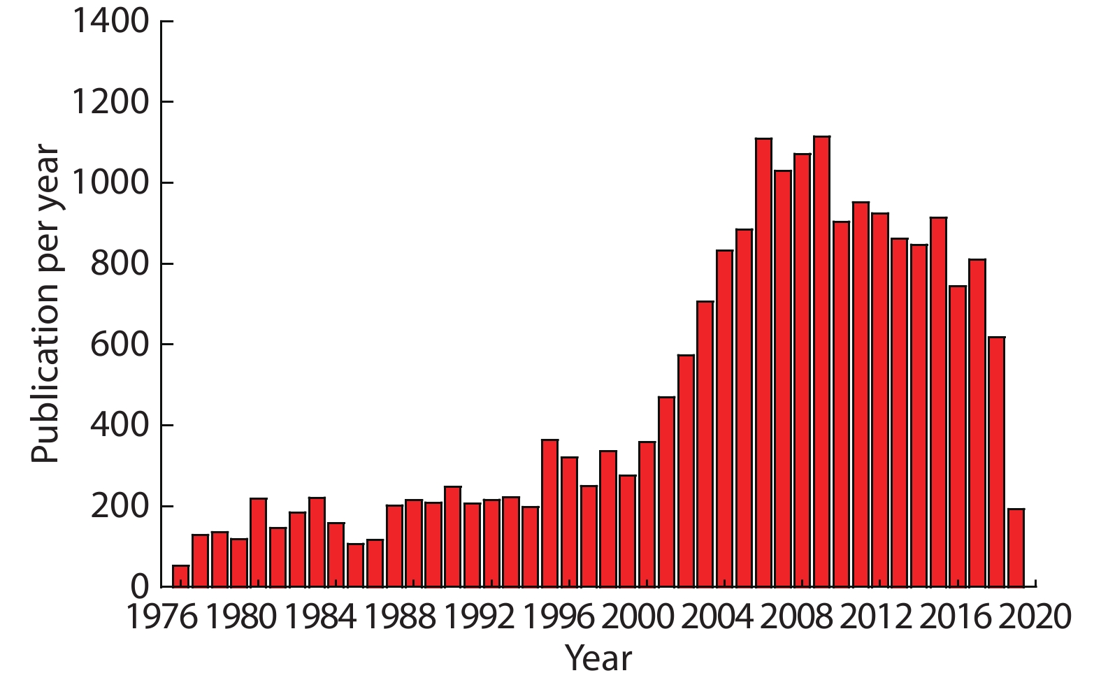
Fig. 1. (Color online) Publications per year on magnetic semiconductors according to the Web of Science. The term “Magnetic semiconductors” was selected as research topic.
![(Color online) (a) Electric field control of the hole-induced ferromagnetism in magnetic semiconductor (In,Mn)As field-effect transistors. (b) Hall resistance versus field curves under three different gate biases. Inset, the same curves shown at higher magnetic fields. Reprinted with permission from Ref. [19]. Copyright (2000) by Springer Nature.](/richHtml/jos/2019/40/8/081501/img_2.jpg)
Fig. 2. (Color online) (a) Electric field control of the hole-induced ferromagnetism in magnetic semiconductor (In,Mn)As field-effect transistors. (b) Hall resistance versus field curves under three different gate biases. Inset, the same curves shown at higher magnetic fields. Reprinted with permission from Ref. [19 ]. Copyright (2000) by Springer Nature.
Fig. 3. (Color online) Electrical spin injection in an epitaxially grown ferromagnetic semiconductor heterostructure based on GaAs. (a) Spontaneous magnitization develops below the Curie temperature T C in the ferromagnetic p-type semiconductor (Ga,Mn)As, depicted by the black arrows in the green layer. Under forward bias, spin-polarized holes from (Ga,Mn)As and unpolarized electrons from the n-type GaAs substrate are injected into the (In,Ga)As quantum well (QW, hatched region), through a spacer layer with thickness d , producing polarized electroluminescence. (b) Hysteretic electroluminescence polarization is a direct result of spin injection from the ferromagnetic (Ga,Mn)As layer. Inset, the relative remanent polarization shown in solid squares at T = 6–94 K. Reprinted with permission from Ref. [20 ]. Copyright (1999) by Springer Nature.
Fig. 4. (Color online) Representation of magnetic polarons. A donor electron in its hydrogenic orbit couples with its spin antiparallel to impurities with a 3d shell that is half-full or more than half-full. Cation sites are represented by small circles. Oxygen is not shown; the unoccupied oxygen sites are represented by squares. Small black balls with arrows represent magnetic ions. Reprinted with permission from Ref. [56 ]. Copyright (2005) by Springer Nature.
Fig. 5. (Color online) (a) Out-of-plane view of the CrI3 structure depicting the Ising spin orientation. (b) Polar MOKE signal for a CrI3 monolayer at a temperature of 15 K. The inset shows an optical image of an isolated monolayer (the scale bar is 2 μ m). Reprinted with permission from Ref. [87 ]. Copyright (2017) by Springer Nature.
Fig. 6. (Color online) (a) Schematic fabrication of (Ga1–x Fex ) Sb thin films. (c)–(i) RHEED patterns taken along the
x Fex ) Sb layers for samples A–G (x = 3.9%−20%, thickness d = 30−100 nm). The RHEED pattern of an undoped GaSb sample is also shown as a reference in (b). Reprinted with permission from Ref. [99 ]. Copyright (2015) by AIP Publishing.
Fig. 7. (Color online) (a) XRD and corresponding RHEED patterns of the Cox Zn1–x O films with x = 0.3, 0.4, and 0.45, respectively. (b)
φ -scans of Co0.4Zn0.6O and Co0.45Zn0.55O films. (c) Experimentally (exp) determined lattice parameters of a/b and c for the Cox Zn1–x O films. The dashed lines are plotted with lattice parameters taken from the reference standards of bulk ZnO and wurtzite CoO[104 ]. (d) Crosssectional scanning TEM image of Co0.45Zn0.55O film. The inset shows a high-resolution TEM image for the same film. Reprinted with permission from Ref. [101 ]. Copyright (2016) by AIP Publishing.
Fig. 8. (Color online) (a) Normalized MR and (b) anomalous Hall resistivity and corresponding M-H loops for the Ga(Co0.4Zn0.6)0.98O film from room temperature down to 5 K. Reprinted with permission from Ref. [102 ]. Copyright (2017) by AIP Publishing.
Fig. 9. (Color online) The schematic band diagrams as s , p -d coupling enhanced by increasing the density of s electrons. Dashed lines denote the Fermi level. Reprinted with permission from Ref. [102 ]. Copyright (2017) by AIP Publishing.
Fig. 10. (a) A low magnification micrograph of Ti0.24Co0.76O2 films and the corresponding electron diffraction pattern in the inset. (b) The high resolution TEM image, and (c) the corresponding elemental mapping of Co. (d) XPS of Co 2p3/2 and Co 2p1/2 peaks. (e) Electron energy-loss spectroscopy of Ti0.24Co0.76O2 films. Reprinted with permission from Ref. [106 ]. Copyright (2006) by AIP Publishing.
Fig. 11. (Color online) Resistivity in logarithmic scale versus T −1/2 for the Zn0.31Co0.69O1−v magnetic semiconductors measured at zero and 5 T magnetic field. Reprinted with permission from Ref. [108 ]. Copyright (2010) by AIP Publishing.
|
Table 1. Composition range and crystal structure of II–VI magnetic semiconductors.


Set citation alerts for the article
Please enter your email address

© Copyright 2018-2021 | Chinese Laser Press. All Rights Reserved 沪ICP备15018463号-20