
Qiang Cao, Shishen Yan. The predicaments and expectations in development of magnetic semiconductors[J]. Journal of Semiconductors, 2019, 40(8): 081501
- Journal of Semiconductors
- Vol. 40, Issue 8, 081501 (2019)
Abstract
1. Introduction
Magnetic semiconductors[
![]()
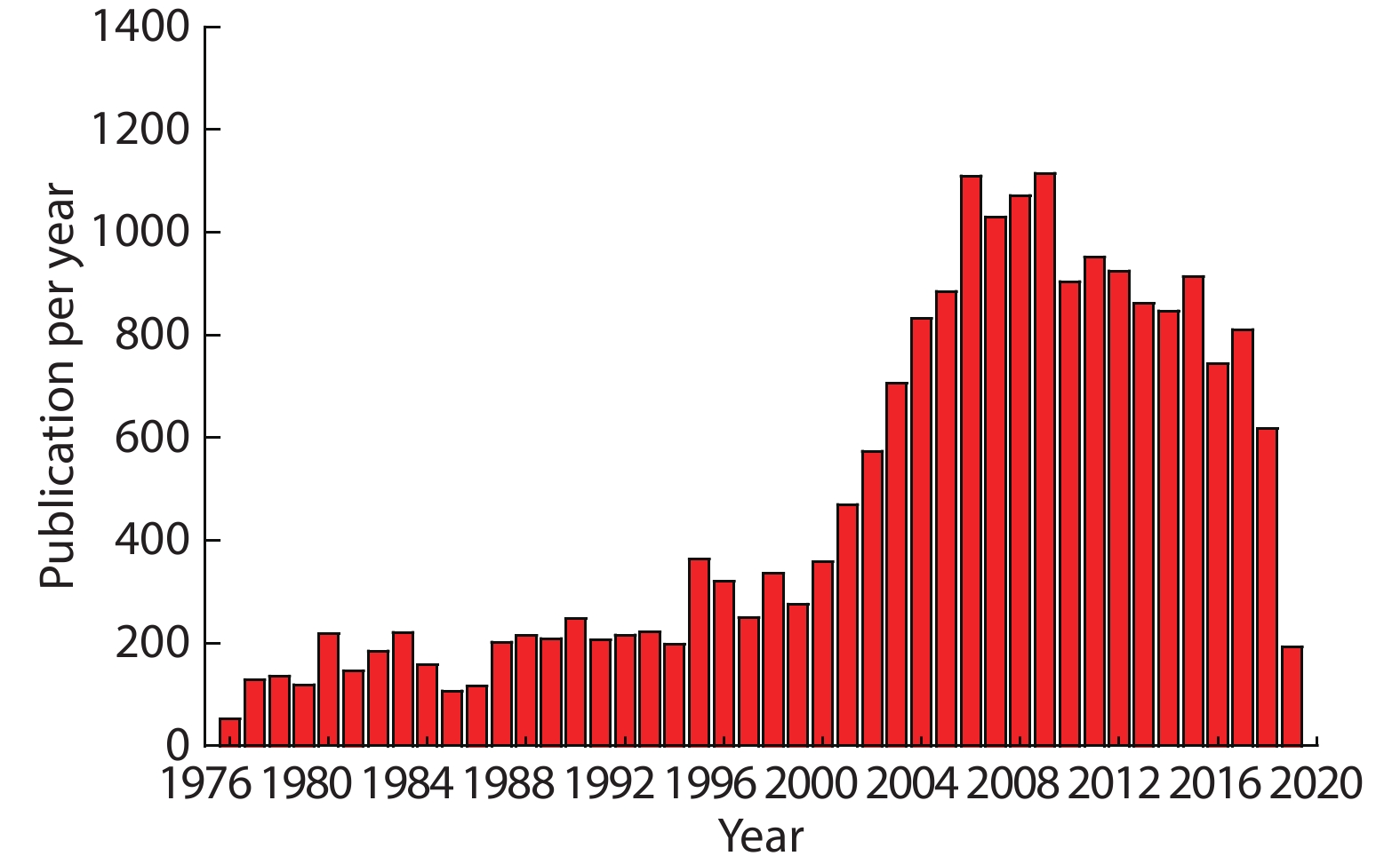
Figure 1.(Color online) Publications per year on magnetic semiconductors according to the Web of Science. The term “Magnetic semiconductors” was selected as research topic.
Despite considerable research efforts, a magnetic semiconductor that exhibits usefully large, gateable spin polarizations at room temperature is still missing[
Unfortunately, neither of them has been demonstrated as a room temperature intrinsic magnetic semiconductor so far. Due to small feasibilities of application, the development of magnetic semiconductors slowed down. In recent years, publications on this subject declined rapidly, as shown in Fig. 1. When a scientific gold-rush excitement passed, it is a good time to think calmly about the ways for seeking room temperature magnetic semiconductors. Here, we would like to quote from Churchill: “This is not the end. It is not even the beginning of the end. But it is, perhaps, the end of the beginning.” Indeed, this is not the first time that the study on magnetic semiconductors sank into a low valley. The question is still open, and a lot of rooms remain for people to exploit. In this review, we will start with a simple historical review to draw inspirations from the past. Then we discuss recent experimental progresses to pursue strong s, p–d interaction to realize room temperature magnetic semiconductors, which are achieved by introducing a very high concentration of magnetic atoms by means of low-temperature nonequilibrium growth.
2. A brief historical perspective on magnetic semiconductors
In history, the list of candidate magnetic semiconductors can be grouped into two categories: undoped magnetic semiconductors, such as europium chalcogenides and semiconducting spinels[
Undoped ferromagnetic semiconductors were extensively studied in the late 1960s to early 1970s. EuO, for example, is considered the first magnetic semiconductor, however, with a low Curie temperature (Tc) of only 77 K[
2.1. II–VI magnetic semiconductors
II–VI compounds (such as CdTe, ZnTe, and CdSe) doped with transition metal (TM) elements (such as Mn) have been studied quite extensively in the 1980s[
2.2. III–V dilute magnetic semiconductors
III–V alloys, such as Ga0.95Mn0.05As, took centre stage in 1996[
![]()
Figure 2.(Color online) (a) Electric field control of the hole-induced ferromagnetism in magnetic semiconductor (In,Mn)As field-effect transistors. (b) Hall resistance versus field curves under three different gate biases. Inset, the same curves shown at higher magnetic fields. Reprinted with permission from Ref. [
![]()
Figure 3.(Color online) Electrical spin injection in an epitaxially grown ferromagnetic semiconductor heterostructure based on GaAs. (a) Spontaneous magnitization develops below the Curie temperature
2.3. Oxide magnetic semiconductors
In April 2000, Tomasz Dietl et al. published a theoretical paper in Science that provided a model to explain the origin of ferromagnetism in (Ga,Mn)As, and used the same model to predict ferromagnetism in wide bandgap materials ZnO and GaN[
![]()
Figure 4.(Color online) Representation of magnetic polarons. A donor electron in its hydrogenic orbit couples with its spin antiparallel to impurities with a 3
Although a considerable amount of experimental data and corresponding mechanisms have been accumulated, the origin and control of ferromagnetism in dilute magnetic oxides are the most controversial research topic in materials science and condensed-matter physics. The data are notoriously plagued by instability and a lack of reproducibility[
2.4. Two dimentional magnetic semiconductors
Since graphene was successfully prepared from graphite in 2004, two dimentional (2D) layered materials have received extensive attentions, which provided new opportunities to make 2D magnetic semiconductors. The first attempt was to add ferromagnetism to the long list of graphene’s capabilities. One can imagine that the ferromagnetic graphene could lead to novel transport phenomena such as the quantized anomalous Hall effect[
The breakthrough of 2D magnetism came in 2017, ferromagnetism was demonstrated in van der Waals (vdW) crystals in the monolayer limit[
![]()
Figure 5.(Color online) (a) Out-of-plane view of the CrI3 structure depicting the Ising spin orientation. (b) Polar MOKE signal for a CrI3 monolayer at a temperature of 15 K. The inset shows an optical image of an isolated monolayer (the scale bar is 2
3. Room temperature magnetic semiconductors with high transitional metal concentration
As a model system, (Ga,Mn)As had provided a good test bed to explore new physics and to design proof-of-concept spintronics devices. So people strived for a new material and transferred the experience with (Ga,Mn)As to it. It is noteworthy that it may be unrealistic if we are committed to find a room temperature dilute magnetic semiconductor with carrier-mediated ferromagnetism just like (Ga,Mn)As. To the best of our knowledge, nobody has demonstrated carrier-mediated ferromagnetism in a dilute magnetic semiconductor at room temperature. The problem is that the s, p–d exchange interaction mediated by free carriers is not large enough in such materials to align local spins ferromagnetically at room temperature, which precludes carrier-mediated ferromagnetism at room temperature in dilute system.
So we discuss a proposal to achieve thermally robust s, p–d interaction in semiconductors. According to the Anderson model[
3.1. Single crystal magnetic semiconductors with high transitional metal concentration
Over the years, the endeavor for improving quality of materials has led to high control of the growth processes. In many cases, low solubility of magnetic elements can be overcame by low-temperature nonequilibrium molecular beam epitaxial (LT-MBE) growth. Recently, (Ga1–xFex) Sb (x = 3.9%−20%) thin films were successfully grown by LT-MBE[
![]()
Figure 6.(Color online) (a) Schematic fabrication of (Ga1–
Another breakthrough was made in Co doped ZnO[
![]()
Figure 7.(Color online) (a) XRD and corresponding RHEED patterns of the Co
![]()
Figure 8.(Color online) (a) Normalized MR and (b) anomalous Hall resistivity and corresponding M-H loops for the Ga(Co0.4Zn0.6)0.98O film from room temperature down to 5 K. Reprinted with permission from Ref. [
The concentration of Co in the films is high enough to exceed the threshold to percolate together and couple close-neighbor local spins to a parallel ground state. Therefore, the ferromagnetism is originated from ferromagnetic p–d coupling between O (2p) and Co (3d) orbitals in the presence of oxygen vacancies. In this regard, the films can be classified as a ferromagnetic insulator, owing to the localized 2p and 3d electrons lying at a deep level within the large band gap of ZnO. By contrast, electronic transport is dominated by s electrons. The polarization of conducting s electron can be very different from the local polarization determined by d electrons. If the s, p–d exchange coupling is very weak, then no spin polarized transport behavior can be observed, as shown in Fig. 9(a). In order to enhance the s, p–d exchange coupling, Ga was introduced to increase the conducting carrier density, because the s, p–d exchange interaction energy depends on the concentration of magnetic ions as well as the density of states of the conducting carrier. By increasing the conducting carrier concentration, the density of states near the Fermi level can be significantly extended into the gap region, which gives rise to more overlapping between the delocalized electronic states (4s) and the localized impurity band (2p and 3d), as shown in Fig. 9(b). As a result, spin-polarized conducting carriers are created, and their density increases with carrier density, owing to the enhancement of s, p–d coupling between Ga (4s), O (2p), and Co (3d) orbitals.
![]()
Figure 9.(Color online) The schematic band diagrams as
3.2. Amorphous and/or nanocrystalline oxide magnetic semiconductors
However, the above dilute magnetic semiconductors and single crystal magnetic semiconductors with relatively high transitional metal concentration are largely limited by their stoichiometry, crystal structure and homogeneity. Beyond these limits, we propose that room temperature semiconductors with high spin-polarization may be realized by preparing amorphous, inhomogeneous and nonstoichiometric materials.
Nanocrystalline Zn1–xCoxO and amorphous Ti1−xCoxO2 magnetic semiconductor films with inhomogeneous composition on the subnanometer scale were prepared by sputtering under thermal nonequilibrium condition[
![]()
Figure 10.(a) A low magnification micrograph of Ti0.24Co0.76O2 films and the corresponding electron diffraction pattern in the inset. (b) The high resolution TEM image, and (c) the corresponding elemental mapping of Co. (d) XPS of Co 2p3/2 and Co 2p1/2 peaks. (e) Electron energy-loss spectroscopy of Ti0.24Co0.76O2 films. Reprinted with permission from Ref. [
One of the most important characters of magnetic semiconductors is the spin polarization. Therefore, a series of wide-band-gap ternary oxide ferromagnetic semiconductor films with high transition metal concentration were prepared to study the spin-polarized transport[
![]()
Figure 11.(Color online) Resistivity in logarithmic scale versus
4. Summary and outlook
It was long held that magnetic semiconductor research was confined to dilute magnetic compounds containing minute amounts of magnetic ions, which leads to a severe limit on its development. However, useful magnetic semiconductors, such as Cd0.55Mn0.45Te[16], may require high concentration of magnetic atoms. Fortunately, a great progress in the epitaxy of semiconductor compounds has made it possible to introduce such a high concentration of dopants without ruining the crystal structure of semiconductor host. A tip of the iceberg for magnetic semiconductors with high magnetic dopants concentration has been emerged. We have a good reason to believe that the magnetic semiconductors with high concentration of magnetic elements will show us new surprise in the years to come.
Acknowledgments
This work was supported by the National Natural Science Foundation of China (Grant Nos. 11434006, and 51871112), the National Basic Research Program of China (Grant No. 2015CB921502), the 111 Project (Grant No. B13029), Shandong Provincial Natural Science Foundation (Grant No. ZR2018MA035).
References
[1] S A Wolf, D D Awschalom, R A Buhrman et al. Spintronics: a spin-based electronics vision for the future. Science, 294, 1488(2001).
[2] K Ando. Seeking Room-temperature ferromagnetic semiconductors. Science, 312, 1883(2006).
[3] A M A J Fabian, C Ertler, P Stano et al. Semiconductor spintronics. Acta Physica Slovaca, 57, 565(2007).
[4] T Jungwirth. Spin-dependent phenomena and device concepts explored in (Ga,Mn)As. Rev Mod Phys, 86, 855(2014).
[5] T Dietl. A ten-year perspective on dilute magnetic semiconductors and oxides. Nat Mater, 9, 965(2010).
[6] S Chambers. Is it really intrinsic ferromagnetism. Nat Mater, 9, 956(2010).
[7] C Seife. Can the laws of physics be unified. Science, 309, 82(2005).
[8] S Chambers, T Droubay, C Wang et al. Ferromagnetism in oxide semiconductors. Mater Today, 9, 28(2006).
[9] A Mauger, C Godart. The magnetic, optical, and transport properties of representatives of a class of magnetic semiconductors: The europium chalcogenides. Phys Rep, 141, 51(1986).
[10] J K Furdyna. Diluted magnetic semiconductors. J Appl Phys, 64, R29(1988).
[11] H Ohno. Making nonmagnetic semiconductors ferromagnetic. Science, 281, 951(1998).
[12] B T Matthias, R M Bozorth, J H Van Vleck. Ferromagnetic interaction in EuO. Phys Rev Lett, 7, 160(1961).
[13] L Zhao, B Zhang, Q Pang et al. Chemical synthesis and magnetic properties of dilute magnetic ZnTe: Cr crystals. Appl Phys Lett, 89, 092111(2006).
[14] T M Pekarek, I Miotkowski, B C Crooker. Magnetic measurements on Cd1–
[15]
[16] A E Turner, R L Gunshor, S Datta. New class of materials for optical isolators. Appl Opt, 22, 3152(1983).
[17] H Ohno, A Shen, F Matsukura et al. (Ga,Mn)As: A new diluted magnetic semiconductor based on GaAs. Appl Phys Lett, 69, 363(1996).
[18] H Wang, L Chen, J Zhao. Enhancement of the Curie temperature of ferromagnetic semiconductor (Ga,Mn)As. Sci Chin Phys, Mechan Astron, 56, 99(2013).
[19] H Ohno, D Chiba, F Matsukura et al. Electric-field control of ferromagnetism. Nature, 408, 944(2000).
[20] Y Ohno, D K Young, B Beschoten et al. Electrical spin injection in a ferromagnetic semiconductor heterostructure. Nature, 402, 790(1999).
[21] V Jeudy, J Curiale, J P Adam et al. Current induced domain wall motion in GaMnAs close to the Curie temperature. J Phys: Conden Matter, 23, 446004(2011).
[22] M Yamanouchi, D Chiba, F Matsukura et al. Current-assisted domain wall motion in ferromagnetic semiconductors. Jpn J Appl Phys, 45, 3854(2006).
[23] A Chernyshov, M Overby, X Liu et al. Evidence for reversible control of magnetization in a ferromagnetic material by means of spin-orbit magnetic field. Nat Phys, 5, 656(2009).
[24] C M Jaworski, J Yang, S Mack et al. Observation of the spin-Seebeck effect in a ferromagnetic semiconductor. Nat Mater, 9, 898(2010).
[25] C M Jaworski, J Yang, S Mack et al. Spin-Seebeck effect: a phonon driven spin distribution. Phys Rev Lett, 106(2011).
[26] H X Tang, R K Kawakami, D D Awschalom et al. Giant planar Hall effect in epitaxial (Ga,Mn)As devices. Phys Rev Lett, 90, 107201(2003).
[27] C Gould, C Rüster, T Jungwirth et al. Tunneling anisotropic magnetoresistance: a spin-valve-like tunnel magnetoresistance using a single magnetic layer. Phys Rev Lett, 93, 117203(2004).
[28] K Olejník, M H S Owen, V. Novák et al. Enhanced annealing, high Curie temperature, and low-voltage gating in (Ga,Mn)As: A surface oxide control study. Phys Rev B, 78, 054403(2008).
[29] L Chen, X Yang, F Yang et al. Enhancing the Curie temperature of ferromagnetic semiconductor (Ga,Mn)As to 200 K via nanostructure engineering. Nano Lett, 11, 2584(2011).
[30] T Dietl, H Ohno, F Matsukura et al. Zener Model description of ferromagnetism in zinc-blende magnetic semiconductors. Science, 287, 1019(2000).
[31] N H Hong, J Sakai, A Hassini. Magnetic properties of V-doped ZnO thin films. J Appl Phys, 97, 10D312(2005).
[32] S Ramachandran, A Tiwari, J Narayan et al. Epitaxial growth and properties of Zn1–
[33] H Saeki, H Tabata, T Kawai. Magnetic and electric properties of vanadium doped ZnO films. Solid State Commun, 120, 439(2001).
[34] M Venkatesan, C B Fitzgerald, J G Lunney et al. Anisotropic ferromagnetism in substituted zinc oxide. Phys Rev Lett, 93, 177206(2004).
[35] N H Hong, J Sakai, N T Huong et al. Role of defects in tuning ferromagnetism in diluted magnetic oxide thin films. Phys Rev B, 72, 045336(2005).
[36] J P Fan, Z Y Quan, X H Xu. Tunable magnetic and transport properties of p-type ZnMnO films with n-type Ga, Cr, and Fe codopants. Appl Phys Lett, 102, 102407(2013).
[37] D C Kundaliya, S B Ogale, S E Lofland et al. On the origin of high-temperature ferromagnetism in the low-temperature-processed Mn–Zn–O system. Nat Mater, 3, 709(2004).
[38] X M Cheng, C L Chien. Magnetic properties of epitaxial Mn-doped ZnO thin films. J Appl Phys, 93, 7876(2003).
[39] P Sharma, A Gupta, K V Rao et al. Ferromagnetism above room temperature in bulk and transparent thin films of Mn-doped ZnO. Nat Mater, 2, 673(2003).
[40] D P Norton, S J Pearton, A F Hebard et al. Ferromagnetism in Mn-implanted ZnO: Sn single crystals. Appl Phys Lett, 82, 239(2003).
[41] S Y Park, P J Kim, Y P Lee et al. Realization of room-temperature ferromagnetism and of improved carrier mobility in Mn-doped ZnO film by oxygen deficiency, introduced by hydrogen and heat treatments. Adv Mater, 19, 3496(2007).
[42] Q Cao, M Fu, G Liu et al. Local vibrational modes competitions in Mn-doped ZnO epitaxial films with tunable ferromagnetism. J Appl Phys, 115, 243906(2014).
[43] X X Wei, C Song, K W Geng et al. Local Fe structure and ferromagnetism in Fe-doped ZnO films. J Phys: Conden Matter, 18, 7471(2006).
[44] G L Liu, Q Cao, J X Deng et al. High
[45] Q Cao, J X Deng, G L Liu et al. Epitaxial properties of Co-doped ZnO thin films grown by plasma assisted molecular beam epitaxy. Chin Phys Lett, 24, 2951(2007).
[46] Q Cao, S He, Y Deng et al. Raman scattering investigations on Co-doped ZnO epitaxial films: Local vibration modes and defect associated ferromagnetism. Curr Appl Phys, 14, 744(2014).
[47] Z Y Chen, Z Q Chen, B Zou et al. Defect mediated ferromagnetism in Ni-doped ZnO nanocrystals evidenced by positron annihilation spectroscopy. J Appl Phys, 112, 083905(2012).
[48] T Wakano, N Fujimura, Y Morinaga et al. Magnetic and magneto-transport properties of ZnO: Ni films. Physica E, 10, 260(2001).
[49] D B Buchholz, R P H Chang, J Y Song et al. Room-temperature ferromagnetism in Cu-doped ZnO thin films. Appl Phys Lett, 87, 082504(2005).
[50] C Sudakar, J S Thakur, G Lawes et al. Ferromagnetism induced by planar nanoscale CuO inclusions in Cu-doped ZnO thin films. Phys Rev B, 75, 054423(2007).
[51] J C A Huang, H S Hsu. Inspection of magnetic semiconductor and clustering structure in CoFe-doped ZnO films by bias-dependent impedance spectroscopy. Appl Phys Lett, 87, 132503(2005).
[52] Y M Cho, W K Choo, H Kim et al. Effects of rapid thermal annealing on the ferromagnetic properties of sputtered Zn1–
[53] D Karmakar, T V C Rao, J V Yakhmi et al. Electronic structure and magnetic properties of (Fe,Co)-codoped ZnO: Theory and experiment. Phys Rev B, 81, 184421(2010).
[54] S Lisenkov, A N Andriotis, R M Sheetz et al. Effects of codoping on the ferromagnetic enhancement in ZnO. Phys Rev B, 83, 235203(2011).
[55] L B Duan, G H Rao, Y C Wang et al. Magnetization and Raman scattering studies of (Co, Mn) codoped ZnO nanoparticles. J Appl Phys, 104, 013909(2008).
[56] J M Coey, M Venkatesan, C B Fitzgerald. Donor impurity band exchange in dilute ferromagnetic oxides. Nat Mater, 4, 173(2005).
[57] T Kaspar, T Droubay, S Heald et al. Hidden ferromagnetic secondary phases in cobalt-doped ZnO epitaxial thin films. Phys Rev B, 77, 201303(R)(2008).
[58] N Jedrecy, H J von Bardeleben, D Demaille. High-temperature ferromagnetism by means of oriented nanocolumns: Co clustering in (Zn,Co)O. Phys Rev B, 80, 205204(2009).
[59] D Zhu, G Liu, Y Tian et al. Decoupled scenario between the conductive carriers and the ferromagnetism in epitaxial Zn0.85–
[60] J W Chiou, H M Tsai, C W Pao et al. Role of valence-band Co 3d states on ferromagnetism in Zn1–
[61] M Kobayashi, Y Ishida, J Hwang et al. Characterization of magnetic components in the diluted magnetic semiconductor Zn1–
[62] . More than just room temperature. Nat Mater, 9, 951(2010).
[63] A Zunger, S Lany, H Raebiger. The quest for dilute ferromagnetism in semiconductors: Guides and misguides by theory. Physics, 3, 53(2010).
[64] C Z Chang, X Feng, J Shen et al. Experimental observation of the quantum anomalous Hall effect in a magnetic topological insulator. Science, 340, 167(2013).
[65] Z Wang, C Tang, R Sachs et al. Proximity-induced ferromagnetism in graphene revealed by the anomalous Hall effect. Phys Rev Lett, 114, 016603(2015).
[66] J Zhou, Q Wang, Q Sun et al. Ferromagnetism in semihydrogenated graphene sheet. Nano Lett, 9, 3867(2009).
[67] D Soriano, N Leconte, P Ordejón et al. Magnetoresistance and magnetic ordering fingerprints in hydrogenated graphene. Phys Rev Lett, 107, 016602(2011).
[68] B Uchoa, V N Kotov, N M R Peres et al. Localized magnetic states in graphene. Phys Rev Lett, 101, 026805(2008).
[69] O V Yazyev. Magnetism in disordered graphene and irradiated graphite. Phys Rev Lett, 101, 037203(2008).
[70] R Faccio, H Pardo, P A Denis et al. Magnetism induced by single carbon vacancies in a three-dimensional graphitic network. Phys Rev B, 77, 035416(2008).
[71] E V Castro, N M R Peres, T Stauber et al. Low-density ferromagnetism in biased bilayer graphene. Phys Rev Lett, 100, 186803(2008).
[72] Y Wang, Y Huang, Y Song et al. Room-temperature ferromagnetism of graphene. Nano Lett, 9, 220(2009).
[73] H S S R Matte, K S Subrahmanyam, C N R Rao. Novel magnetic properties of graphene: presence of both ferromagnetic and antiferromagnetic features and other aspects. J Phys Chem C, 113, 9982(2009).
[74] L Xie, X Wang, J Lu et al. Room temperature ferromagnetism in partially hydrogenated epitaxial graphene. Appl Phys Lett, 98, 193113(2011).
[75] A Candini, C Alvino, W Wernsdorfer et al. Hysteresis loops of magnetoconductance in graphene devices. Phys Rev B, 83, 121401(2011).
[76] M Sepioni, R R Nair, S Rablen et al. Limits on intrinsic magnetism in graphene. Phys Rev Lett, 105, 207205(2010).
[77] R R Nair, M Sepioni, I L Tsai et al. Spin-half paramagnetism in graphene induced by point defects. Nat Phys, 8, 199(2012).
[78] H Zhang, M Chhowalla, Z Liu. 2D nanomaterials: graphene and transition metal dichalcogenides. Chem Soc Rev, 47, 3015(2018).
[79] X Wang, Z Song, W Wen et al. Potential 2D materials with phase transitions: structure, synthesis, and device applications. Adv Mater, 1804682(2018).
[80] J Shi, M Hong, Z Zhang et al. Physical properties and potential applications of two-dimensional metallic transition metal dichalcogenides. Coord Chem Rev, 376, 1(2018).
[81] A Ramasubramaniam, D Naveh. Mn-doped monolayer MoS2: An atomically thin dilute magnetic semiconductor. Phys Rev B, 87, 195201(2013).
[82] R Mishra, W Zhou, S J Pennycook et al. Long-range ferromagnetic ordering in manganese-doped two-dimensional dichalcogenides. Phys Rev B, 88, 144409(2013).
[83] L Sun, W Zhou, Y Liang et al. Magnetic properties in Fe-doped SnS2: Density functional calculations. Comput Mater Sci, 117, 489(2016).
[84] L Seixas, A Carvalho, A H Castro Neto. Atomically thin dilute magnetism in Co-doped phosphorene. Phys Rev B, 91, 155138(2015).
[85] B Li, T Xing, M Zhong et al. A two-dimensional Fe-doped SnS2 magnetic semiconductor. Nat Commun, 8, 1958(2017).
[86] C Gong, L Li, Z Li et al. Discovery of intrinsic ferromagnetism in two-dimensional van der Waals crystals. Nature, 546, 265(2017).
[87] B Huang, G Clark, N Moratalla et al. Layer-dependent ferromagnetism in a van der Waals crystal down to the monolayer limit. Nature, 546, 270(2017).
[88] R B Griffiths. Peierls proof of spontaneous magnetization in a two-dimensional ising ferromagnet. Phys Rev, 136, A437(1964).
[89] N D Mermin, H Wagner. Absence of ferromagnetism or antiferromagnetism in one- or two-dimensional isotropic heisenberg models. Phys Rev Lett, 17, 1133(1966).
[90] Z Wang, T Zhang, M Ding et al. Electric-field control of magnetism in a few-layered van der Waals ferromagnetic semiconductor. Nat Nanotechnol, 13, 554(2018).
[91] S Jiang, J Shan, K F Mak. Electric-field switching of two-dimensional van der Waals magnets. Nat Mater, 17, 406(2018).
[92] S Jiang, L Li, Z Wang et al. Controlling magnetism in 2D CrI3 by electrostatic doping. Nat Nanotechnol, 13, 549(2018).
[93] B Huang, G Clark, D R Klein et al. Electrical control of 2D magnetism in bilayer CrI3. Nat Nanotechnol, 13, 544(2018).
[94] P W Anderson. Localized magnetic states in metals. Phys Rev, 124, 41(1961).
[95] J R Schrieffer, P A Wolff. Relation between the Anderson and Kondo Hamiltonians. Phys Rev, 149, 491(1966).
[96] A H MacDonald, P Schiffer, N Samarth. Ferromagnetic semiconductors: moving beyond (Ga,Mn)As. Nat Mater, 4, 195(2005).
[97] Y J Zeng, N Gauquelin, D Y Li et al. Co-rich ZnCoO nanoparticles embedded in wurtzite Zn1–
[98] K Akaiwa, K Kaneko, S Fujita et al. Room temperature ferromagnetism in conducting α-(In1–
[99] N T Tu, P N Hai, L D Anh et al. Magnetic properties and intrinsic ferromagnetism in (Ga,Fe)Sb ferromagnetic semiconductors. Phys Rev B, 92, 144403(2015).
[100] L Li, Y Guo, X Y Cui et al. Magnetism of Co-doped ZnO epitaxially grown on a ZnO substrate. Phys Rev B, 85, 174430(2012).
[101] Q Cao, D Zhu, M Fu et al. Robust ferromagnetism of single crystalline Co
[102] Q Cao, M Fu, D Zhu et al. Enhancing s,
[103] Q Cao, M Fu, D Zhu et al. Growth-controlled engineering of magnetic exchange interactions in single crystalline GaCo- ZnO1–v epitaxial films with high Co concentration. Chem Mater, 29, 2717(2017).
[104] M J Redman, E G Steward. Cobaltous oxide with the zinc blende/wurtzite-type crystal structure. Nature, 193, 867(1962).
[105] S S Yan, C Ren, X Wang et al. Ferromagnetism and magnetoresistance of Co–ZnO inhomogeneous magnetic semiconductor. Appl Phys Lett, 84, 2376(2004).
[106] H Q Song, L M Mei, S S Yan et al. Microstructure, ferromagnetism, and magnetic transport of Ti1–
[107] S S Yan, J P Liu, L M Mei et al. Spin-dependent variable range hopping and magnetoresistance in Ti1–
[108] Y F Tian, S S Yan, M W Zhao et al. Controllable spin- polarized electrical transport in wide-band-gap oxide ferromagnetic semiconductors. J Appl Phys, 107, 033713(2010).

Set citation alerts for the article
Please enter your email address
© Copyright 2018-2021 | Chinese Laser Press. All Rights Reserved 沪ICP备15018463号-20