• Photonics Research
  • Vol. 6, Issue 2, 109 (2018)
Miaofeng Li1、2、3, Lei Wang2、3, Xiang Li2、3, Xi Xiao2、3、*, and Shaohua Yu1、2、3
Author Affiliations
  • 1Wuhan National Laboratory for Optoelectronics, School of Optical and Electronic Information, Huazhong University of Science and Technology, Wuhan 430074, Hubei, China
  • 2State Key Laboratory of Optical Communication Technologies and Networks, Wuhan Research Institute of Posts & Telecommunications, Wuhan 430074, Hubei, China
  • 3National Information Optoelectronics Innovation Center, Wuhan 430074, Hubei, China
  • show less
    DOI: 10.1364/PRJ.6.000109 Cite this Article Set citation alerts
    Miaofeng Li, Lei Wang, Xiang Li, Xi Xiao, Shaohua Yu. Silicon intensity Mach–Zehnder modulator for single lane 100  Gb/s applications[J]. Photonics Research, 2018, 6(2): 109 Copy Citation Text show less
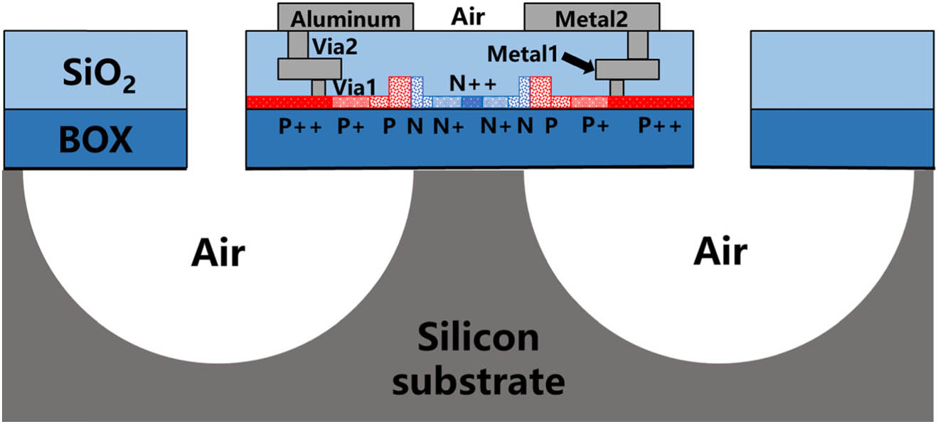
    Diagram of the cross-sectional structure.
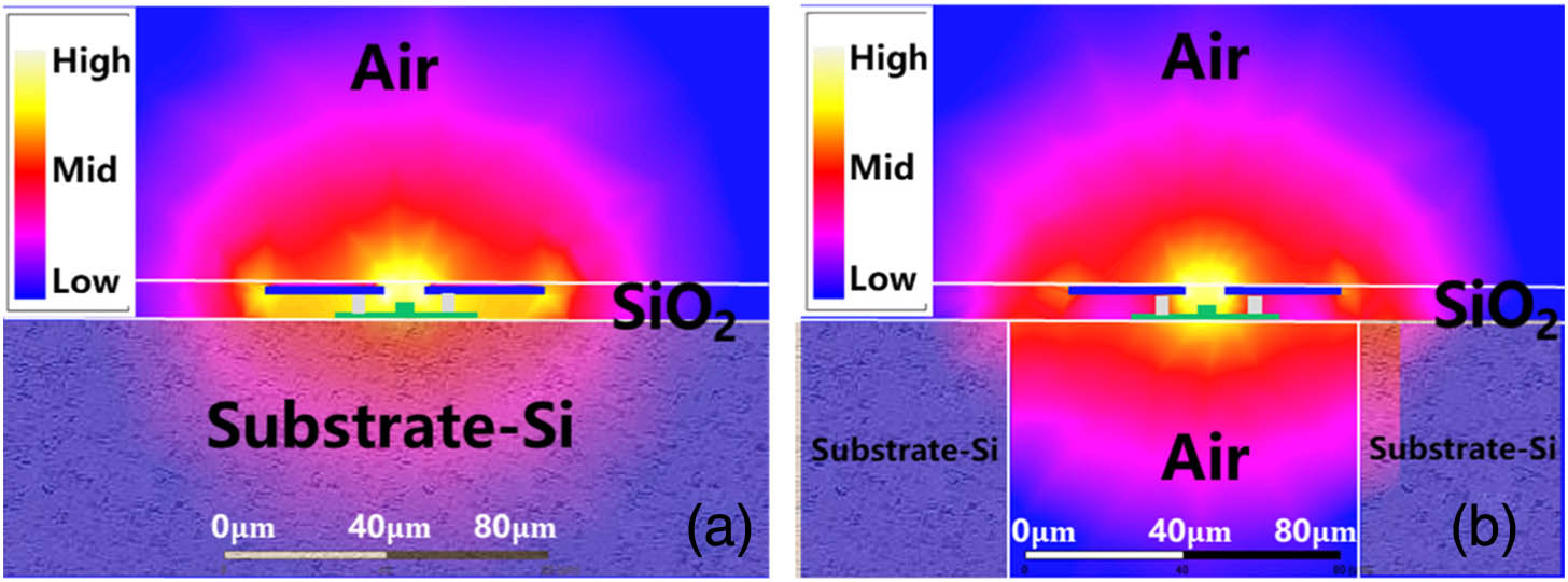
    Fig. 1. Diagram of the cross-sectional structure.
    Microwave electrical mode distribution of the TWMZM cross section (a) before and (b) after the silicon substrate is removed.
    Fig. 2. Microwave electrical mode distribution of the TWMZM cross section (a) before and (b) after the silicon substrate is removed.
    Microwave attenuation based on finite element method (FEM) simulations on unloaded CPS transmission lines before and after substrate removing of the wafer used in our design.
    Fig. 3. Microwave attenuation based on finite element method (FEM) simulations on unloaded CPS transmission lines before and after substrate removing of the wafer used in our design.
    Simulated EO S21 before and after substrate removal of the wafer used in our design.
    Fig. 4. Simulated EO S21 before and after substrate removal of the wafer used in our design.
    Fabrication process of the substrate removed modulator based on IME’s silicon photonics platform.
    Fig. 5. Fabrication process of the substrate removed modulator based on IME’s silicon photonics platform.
    Micrograph of the fabricated substrate removed silicon modulator viewed from above and the enlarged picture of the (a) edge couple, (b) phase shifter, and (c) the electrode region.
    Fig. 6. Micrograph of the fabricated substrate removed silicon modulator viewed from above and the enlarged picture of the (a) edge couple, (b) phase shifter, and (c) the electrode region.
    (a) Measured EE S21 of the substrate removed modulator under various bias voltages. (b) Microwave index of the modulator before and after the silicon substrate is removed, which is extracted from the tested EE S21 at −4 V bias voltage. (c) Electrode characteristic impedance of the modulator before and after the silicon substrate is removed, which is calculated from the tested EE S21 and S11 at −4 V bias voltage.
    Fig. 7. (a) Measured EE S21 of the substrate removed modulator under various bias voltages. (b) Microwave index of the modulator before and after the silicon substrate is removed, which is extracted from the tested EE S21 at 4  V bias voltage. (c) Electrode characteristic impedance of the modulator before and after the silicon substrate is removed, which is calculated from the tested EE S21 and S11 at 4  V bias voltage.
    Measured EO S21 response under various bias voltages after the silicon substrate is removed.
    Fig. 8. Measured EO S21 response under various bias voltages after the silicon substrate is removed.
    Experimental setup for the substrate removed TWMZM OOK eye-diagram measurements.
    Fig. 9. Experimental setup for the substrate removed TWMZM OOK eye-diagram measurements.
    Optical eye diagrams at the different rates of 70 GBaud/s, 80 GBaud/s, and 90 GBaud/s under the driving voltage of 5 V Vpp without any pre-emphasis under bias voltage of −6 V. The extinction ratios are 3.6 dB, 2.7 dB, and 3.3 dB, respectively.
    Fig. 10. Optical eye diagrams at the different rates of 70  GBaud/s, 80  GBaud/s, and 90  GBaud/s under the driving voltage of 5 V Vpp without any pre-emphasis under bias voltage of 6  V. The extinction ratios are 3.6 dB, 2.7 dB, and 3.3 dB, respectively.
    Experimental setup for the substrate removed TWMZM PAM-4 eye-diagram measurements.
    Fig. 11. Experimental setup for the substrate removed TWMZM PAM-4 eye-diagram measurements.
    Measured PAM-4 modulation optical eye diagrams at 28 GBaud/s, 50 GBaud/s, and 56 GBaud/s without any pre-emphasis under bias voltage of −6 V. The extinction ratios are 3.6 dB, 2.5 dB, and 2.7 dB, respectively.
    Fig. 12. Measured PAM-4 modulation optical eye diagrams at 28  GBaud/s, 50  GBaud/s, and 56  GBaud/s without any pre-emphasis under bias voltage of 6  V. The extinction ratios are 3.6 dB, 2.5 dB, and 2.7 dB, respectively.
    Experimental setup for the PAM-4 signal transmission based on the substrate removed silicon modulator even different distances.
    Fig. 13. Experimental setup for the PAM-4 signal transmission based on the substrate removed silicon modulator even different distances.
    Measured curve of BER versus the received optical power for 56 GBaud/s (112 Gb/s) PAM-4 signal transmission under bias voltage of −6 V.
    Fig. 14. Measured curve of BER versus the received optical power for 56  GBaud/s (112  Gb/s) PAM-4 signal transmission under bias voltage of 6  V.
    Measured curve of BER versus the received optical power for 64 GBaud/s (128 Gb/s) PAM-4 signal transmission under bias voltage of −6 V.
    Fig. 15. Measured curve of BER versus the received optical power for 64  GBaud/s (128  Gb/s) PAM-4 signal transmission under bias voltage of 6  V.
    Miaofeng Li, Lei Wang, Xiang Li, Xi Xiao, Shaohua Yu. Silicon intensity Mach–Zehnder modulator for single lane 100  Gb/s applications[J]. Photonics Research, 2018, 6(2): 109
    Download Citation