Weisheng Li, Hongkai Ning, Zhihao Yu, Yi Shi, Xinran Wang. Reducing the power consumption of two-dimensional logic transistors[J]. Journal of Semiconductors, 2019, 40(9): 091002
Search by keywords or author
- Journal of Semiconductors
- Vol. 40, Issue 9, 091002 (2019)
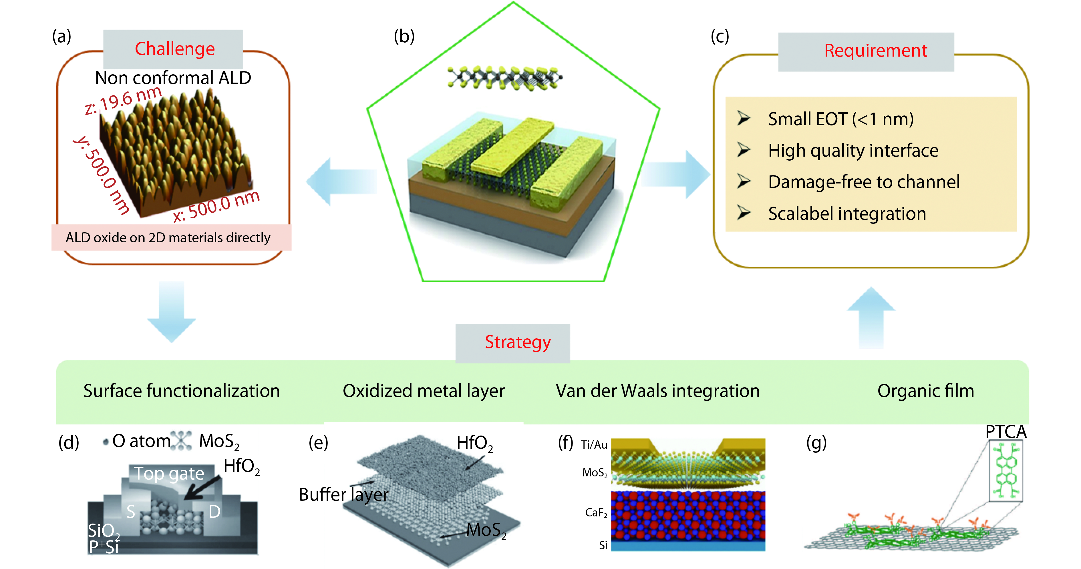
![(Color online) Integrating ultra-thin high-κ dielectric on 2D materials. (a) The 3D AFM image of HfO2 deposited directly on MoS2 by ALD technique forms an island structure[26]. (b) Schematic of top gate FET based on monolayer 2D TMDC[7]. (c) Requirement of high-κ dielectric on 2D materials for low power device; (d) Device schematic of the top-gated MoS2 FET with HfO2 dielectric deposited by ozone pretreatment[31]. (e) Structural schematic of few layer MoS2 covered with the metal oxide buffer layer and HfO2 film[33]. (f) Illustration of the atomic structure of the bilayer MoS2 FETs with a CaF2 gate dielectric[35]. A quasi-van der Waals interface is formed between the F-terminated CaF2 (111) and the MoS2 channel. (g) PTCA coated graphene. PTCA selectively adheres to graphene on SiO2 surfaces, providing binding sites for ALD deposition. Inset is a top view of PTCA structure[38].](/richHtml/jos/2019/40/9/091002/img_1.jpg)
Fig. 1. (Color online) Integrating ultra-thin high-κ dielectric on 2D materials. (a) The 3D AFM image of HfO2 deposited directly on MoS2 by ALD technique forms an island structure[26 ]. (b) Schematic of top gate FET based on monolayer 2D TMDC[7 ]. (c) Requirement of high-κ dielectric on 2D materials for low power device; (d) Device schematic of the top-gated MoS2 FET with HfO2 dielectric deposited by ozone pretreatment[31 ]. (e) Structural schematic of few layer MoS2 covered with the metal oxide buffer layer and HfO2 film[33 ]. (f) Illustration of the atomic structure of the bilayer MoS2 FETs with a CaF2 gate dielectric[35 ]. A quasi-van der Waals interface is formed between the F-terminated CaF2 (111) and the MoS2 channel. (g) PTCA coated graphene. PTCA selectively adheres to graphene on SiO2 surfaces, providing binding sites for ALD deposition. Inset is a top view of PTCA structure[38 ].
![(Color online) Basic concept of NC and ultra-low power NCFETs based on 2D TMDC. (a) Schematic of two capacitors in series. Vint is the voltage at the interface, equaling to the radio of gate voltage V and body factor m. (b) Gibb’s free energy-polarization (U–P) diagram[58] of FE, DE, and a series of them for capacitance matching and stabilization of negative capacitance. (c) Polarization–Voltage (P–V) curves deducted from U–P curves in (b). An S-shaped curve of FE is shown. (d) Polarization–electric field (P–E) loop of ferroelectric HZO and the schematic of back gate MoS2 NCFETs. (e) ID–VGS curves of a MoS2 NCFET[16] on 4 nm AL2O3/20 nm HZO (black: forward sweep, red: reverse sweep, grey: gate leakage) and control device with the same channel length of 1.7 μm on 25 nm Al2O3 (blue) at VDS = 0.1 V. (f) A brief summary of representative SS-hysteresis data of reported 2D NCFETs, including MoS2 FETs with HZO[16, 18, 54, 55], PVDF[59], CIPs[60, 61], and WSe2 FETs with HZO dielectric[56, 57], while three typical works based on Si are selected for comparation. According to ITRS 2.0[6], the requirements for scaled SS, 40 mV/dec in 2024, 25 mV/dec in 2030, are plotted respectively.](/richHtml/jos/2019/40/9/091002/img_2.jpg)
Fig. 2. (Color online) Basic concept of NC and ultra-low power NCFETs based on 2D TMDC. (a) Schematic of two capacitors in series. V int is the voltage at the interface, equaling to the radio of gate voltage V and body factor m . (b) Gibb’s free energy-polarization (U–P ) diagram[58 ] of FE, DE, and a series of them for capacitance matching and stabilization of negative capacitance. (c) Polarization–Voltage (P–V ) curves deducted from U–P curves in (b). An S-shaped curve of FE is shown. (d) Polarization–electric field (P–E ) loop of ferroelectric HZO and the schematic of back gate MoS2 NCFETs. (e) I D–V GS curves of a MoS2 NCFET[16 ] on 4 nm AL2O3/20 nm HZO (black: forward sweep, red: reverse sweep, grey: gate leakage) and control device with the same channel length of 1.7 μ m on 25 nm Al2O3 (blue) at V DS = 0.1 V. (f) A brief summary of representative SS-hysteresis data of reported 2D NCFETs, including MoS2 FETs with HZO[16 , 18 , 54 , 55 ], PVDF[59 ], CIPs[60 , 61 ], and WSe2 FETs with HZO dielectric[56 , 57 ], while three typical works based on Si are selected for comparation. According to ITRS 2.0[6 ], the requirements for scaled SS, 40 mV/dec in 2024, 25 mV/dec in 2030, are plotted respectively.

Set citation alerts for the article
Please enter your email address


