[1] K Lange, G Müller-Seitz, J Sydow et al. Financing innovations in uncertain networks—Filling in roadmap gaps in the semiconductor industry. Research Policy, 42, 647(2013).
[2] M M Waldrop. The chips are down for Moore’s law. Nat News, 530, 144(2016).
[3] W Liu, J Kang, W Cao et al. High-performance few-layer-MoS2 field-effect-transistor with record low contact-resistance. IEEE International Electron Devices Meeting, 19(2013).
[4] C Martin. Towards a new scale. Nat Nanotechnol, 11, 112(2016).
[5] D Kwon, K Chatterjee, A J Tan et al. Improved subthreshold swing and short channel effect in FDSOI n-channel negative capacitance field effect transistors. IEEE Electron Device Lett, 39, 300(2017).
[6]
[7] B Radisavljevic, A Radenovic, J Brivio et al. Single-layer MoS2 transistors. Nat Nanotechnol, 6, 147(2011).
[8] H Liu, A T Neal, P D Ye. Channel length scaling of MoS2 MOSFETs. ACS Nano, 6, 8563(2012).
[9] S B Desai, S R Madhvapathy, A B Sachid et al. MoS2 transistors with 1-nanometer gate lengths. Science, 354, 99(2016).
[10] K Alam, R K Lake. Monolayer MoS2 transistors beyond the technology road map. IEEE Trans Electron Devices, 59, 3250(2012).
[11] Q H Wang, K Kalantar-Zadeh, A Kis et al. Electronics and optoelectronics of two-dimensional transition metal dichalcogenides. Nat Nanotechnol, 7, 699(2012).
[12] Z Yu, Z Y Ong, S Li et al. Analyzing the carrier mobility in transition-metal dichalcogenide MoS2 field-effect transistors. Adv Fun Mater, 27, 1604093(2017).
[13] G Fiori, F Bonaccorso, G Iannaccone et al. Electronics based on two-dimensional materials. Nat Nanotechnol, 9, 768(2014).
[14] M Chhowalla, D Jena, H Zhang. Two-dimensional semiconductors for transistors. Nat Rev Mater, 1, 16052(2016).
[15]
[16] Z Yu, H Wang, W Li et al. Negative capacitance 2D MoS2 transistors with sub-60 mV/dec subthreshold swing over 6 orders, 250
[17] S Salahuddin, S Dattat. Use of negative capacitance to provide voltage amplification for low power nanoscale devices. Nano Lett, 8, 405(2008).
[18] M Si, C J Su, C Jiang et al. Steep-slope hysteresis-free negative capacitance MoS2 transistors. Nat Nanotechnol, 13, 24(2018).
[19] F J Himpsel, F R McFeely, A Taleb-Ibrahimi et al. Microscopic structure of the SiO2/Si interface. Phys Rev B, 38, 6084(1988).
[20] J Robertson. High dielectric constant oxides. Eur Phys J-Appl Phys, 28, 265(2004).
[21] J Robertson. High dielectric constant gate oxides for metal oxide Si transistors. Rep Prog Phys, 69, 327(2005).
[22] C Auth, A Cappellani, J S Chun et al. In 45 nm high
[23] S M George. Atomic layer deposition: an overview. Chem Rev, 110, 111(2009).
[24] P J Cowdery-Corvan, D H Levy, S F Nelson et al. Process for atomic layer deposition. Google Patents(2012).
[25] Z Krivokapic, U Rana, R Galatage et al. 14 nm ferroelectric FinFET technology with steep subthreshold slope for ultra low power applications. IEEE International Electron Devices Meeting (IEDM), 15.1.1(2017).
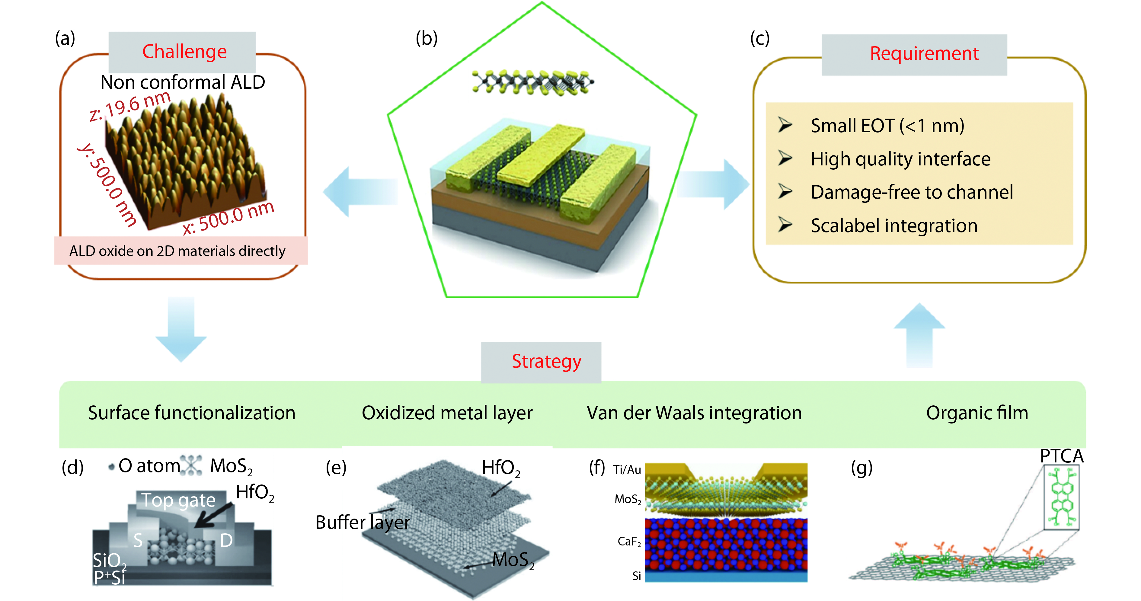
[26] S McDonnell, B Brennan, A Azcatl et al. HfO2 on MoS2 by atomic layer deposition: adsorption mechanisms and thickness scalability. ACS Nano, 7, 10354(2013).
[27] J Yang, S Kim, W Choi et al. Improved growth behavior of atomic-layer-deposited high-
[28] W Yang, Q Q Sun, Y Geng et al. The integration of sub-10 nm gate oxide on MoS2 with ultra low leakage and enhanced mobility. Sci Rep, 5, 11921(2015).
[29] A Azcatl, K Santosh, X Peng et al. HfO2 on UV–O3 exposed transition metal dichalcogenides: interfacial reactions study. 2D Mater, 2, 014004(2015).
[30] A Azcatl, S McDonnell, K C Santosh et al. MoS2 functionalization for ultra-thin atomic layer deposited dielectrics. Appl Phys Lett, 104, 111601(2014).
[31] J Wang, S Li, X Zou et al. Integration of high-
[32] M Xiao, C Qiu, Z Zhang et al. Atomic-layer-deposition growth of an ultrathin HfO2 film on graphene. ACS Appl Mater Interfaces, 9, 34050(2017).
[33] X Zou, J Wang, C H Chiu et al. Interface engineering for high-performance top-gated MoS2 field-effect transistors. Adv Mater, 26, 6255(2014).
[34] N Takahashi, K Nagashio. Buffer layer engineering on graphene via various oxidation methods for atomic layer deposition. Appl Phys Express, 9, 125101(2016).
[35] Y Y Illarionov, A G Banshchikov, D K Polyushkin et al. Ultrathin calcium fluoride insulators for two-dimensional field-effect transistors. Nat Electron, 2, 230(2019).
[36] L Liao, Y C Lin, M Bao et al. High-speed graphene transistors with a self-aligned nanowire gate. Nature, 467, 305(2010).
[37] L Liao, J Bai, Y Qu et al. High-
[38] X Wang, S M Tabakman, H Dai. Atomic layer deposition of metal oxides on pristine and functionalized graphene. J Am Chem Soc, 130, 8152(2008).
[39] J M Alaboson, Q H Wang, J D Emery et al. Seeding atomic layer deposition of high-
[40] V K Sangwan, D Jariwala, S A Filippone et al. Quantitatively enhanced reliability and uniformity of high-
[41] J H Park, S Fathipour, I Kwak et al. Atomic layer deposition of Al2O3 on WSe2 functionalized by titanyl phthalocyanine. ACS Nano, 10, 6888(2016).
[42] B Jiang, Z Y Yang, X Q Liu et al. Interface engineering for two-dimensional semiconductor transistors. Nano Today, 25, 122(2019).
[43] H G Kim, H B R Leek. Atomic layer deposition on 2D materials. Chem Mater, 29, 3809(2017).
[44]
[45] A I Khan, K Chatterjee, B Wang et al. Negative capacitance in a ferroelectric capacitor. Nat Mater, 7, 182(2015).
[46] M Hoffmann, M Pešić, K Chatterjee et al. Direct observation of negative capacitance in polycrystalline ferroelectric HfO2. Adv Funct Mater, 26, 8643(2016).
[47] M Hoffmann, F P Fengler, M Herzig et al. Unveiling the double-well energy landscape in a ferroelectric layer. Nature, 565, 464(2019).
[48] J Müller, T S Böscke, U Schröder et al. Ferroelectricity in simple binary ZrO2 and HfO2. Nano Lett, 12, 4318(2012).
[49] C H Cheng, A Chin. Low-voltage steep turn-on pMOSFET using ferroelectric high-
[50] M H Lee, S T Fan, C H Tang et al. Physical thickness 1.x nm ferroelectric HfZrO
[51] C C Li, K S Chang-Liao, L J Liu et al. Improved electrical characteristics of Ge MOS devices with high oxidation state in HfGeO
[52] J Zhou, G Han et al. Ferroelectric HfZrO
[53] M H Lee, P G Chen, C Liu et al. Prospects for ferroelectric HfZrO
[54] M Si, C Jiang, C J Su et al. Sub-60 mV/dec ferroelectric HZO MoS2 negative capacitance field-effect transistor with internal metal gate: the role of parasitic capacitance. IEEE International Electron Devices Meeting (IEDM), 23.5.1(2017).
[55] F A McGuire, Y C Lin, K Price et al. Sustained sub-60 mV/decade switching via the negative capacitance effect in MoS2 transistors. Nano Lett, 17, 4801(2017).
[56] M Si, C Jiang, W Chung et al. Steep-slope WSe2 negative capacitance field-effect transistor. Nano Lett, 18, 6(2018).
[57] J Wang, X Guo, Z Yu et al. Steep slope p-type 2D WSe2 field-effect transistors with van der waals contact and negative capacitance. IEEE International Electron Devices Meeting (IEDM), 22.3.1(2018).
[58] H W Park, J Roh, Y B Lee et al. Modeling of negative capacitance in ferroelectric thin films. Adv Mater, 1805266(2019).
[59] X Wang, Y Chen, G Wu et al. Two-dimensional negative capacitance transistor with polyvinylidene fluoride-based ferroelectric polymer gating. npj 2D Mater Appl, 1, 38(2017).
[60] X Wang, P Yu, Z Lei et al. Van der Waals negative capacitance transistors. Nat Commun, 10, 3037(2019).
[61] M W Si, P Y Liao, G Qiu et al. Ferroelectric field-effect transistors based on MoS2 and CuInP2S6 two-dimensional van der Waals heterostructure. ACS Nano, 12, 7(2018).
[62] J Müller, T S Böscke, S Müller et al. Ferroelectric hafnium oxide: a CMOS-compatible and highly scalable approach to future ferroelectric memories. IEEE International Electron Devices Meeting (IEDM), 10, 10.8.1(2013).
[63] T Shimizu, T Yokouchi, T Oikawa et al. Contribution of oxygen vacancies to the ferroelectric behavior of Hf0.5Zr0.5O2 thin films. Appl Phys Lett, 106, 112904(2015).