
Weisheng Li, Hongkai Ning, Zhihao Yu, Yi Shi, Xinran Wang. Reducing the power consumption of two-dimensional logic transistors[J]. Journal of Semiconductors, 2019, 40(9): 091002
- Journal of Semiconductors
- Vol. 40, Issue 9, 091002 (2019)
Abstract
1. Introduction
The gradual geometrical scale down of logic devices has successfully approached the ultimate performance of silicon transistors in the past 60 years[
2D semiconductors, especially transition metal dichalcogenides (TMDC), have a satisfied thickness-dependent bandgap of 1–2 eV, which can enable lots of fascinating device applications in field-effect transistors (FETs) with the extraordinary on/off current ratio (> 108) and off-state current (< 1 pA), and atomically thin body thickness, which gives new opportunities to improve gate control and reduce the SCE main issues in ultra-scaled devices[
The static and dynamic power consumption of logic transistors are proportional to operating voltage (Vdd) and quadratic of Vdd, respectively[
According to the Boltzmann tyranny, the SS of MOSFETs at room temperature will not be lower than
Here, we will summarize the latest progress of 2D low-power logic transistors from the following aspects. First, we will give a brief discussion of the ultra-thin dielectric integration on 2D TMDC, together with analysis of interface quality from different interface passivation. Then, novel NCFETs will be discussed, including the working mechanism and device progress. Moreover, a perspective for sub-1 nm EOT and NCFETs will be discussed in the last paragraph of the corresponding section.
2. Integration of ultrathin dielectric on 2D materials
In the early days of the semiconductor industry, SiO2 has been used as a gate dielectric of MOSFETs for decades due to nearly ideal interface between Si and SiO2[
So far, the most controllable approach in semiconductor industry for low cost, high-quality, scalable dielectric deposition is atomic layer deposition (ALD)[
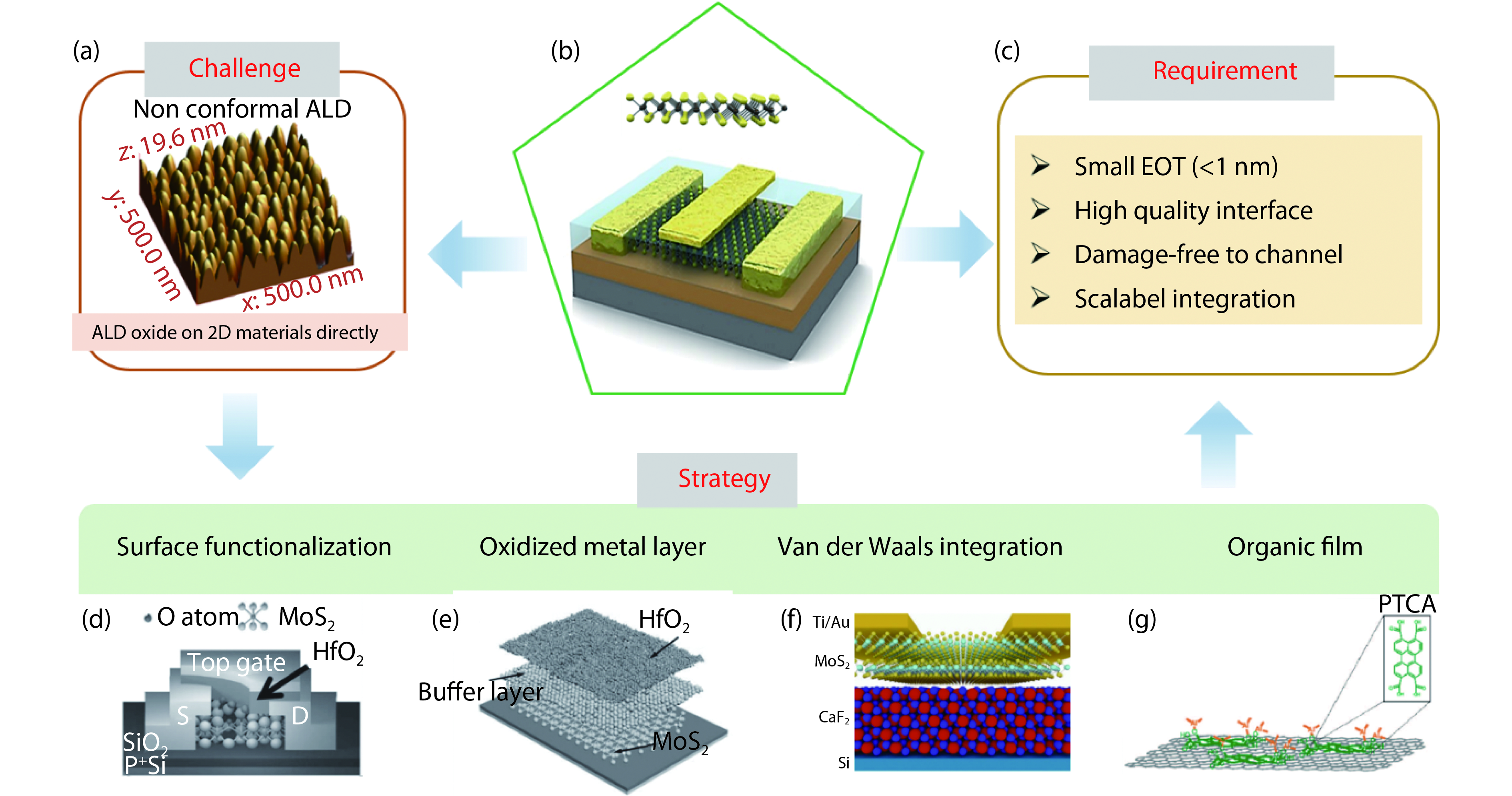
![]()
Figure 1.(Color online) Integrating ultra-thin high-
The surface of 2D material is pretreated by high-activity units such as plasma, ozone and electron beam to increase the nucleation sites for ALD. However, these processes involve high-energy and reactive species which will introduce the overmuch defects and interface states[
Besides, using organic film as the seeding layer to realize the conformal deposition of oxide on 2D materials, which is more amicable than the above surface functionalization and oxidized metal layer method to 2D materials because of ultra-smooth interface of organic crystal and damage-free van der Waals interaction[
Although some new techniques applied, compared with the advanced technology, high-κ dielectric with larger EOT and inferior interface quality are still one of the biggest obstacles to the application of 2D MOSFETs. Fig. 1(c) shows the requirement of high-quality dielectric on 2D materials, including smaller EOT and Dit, potential of scalable integration and so on. The organic seeding layer is one of the most promising techniques for implementing large-scale 2D integrated circuits due to damage-free interface and scalable integration potential, which are the great advantages beyond other technologies. Recent developments indicate that some organic molecules can self-limited assemble on 2D materials by van der Waals interaction with thickness of only single atomic layer[
3. Ultra-low power NC-FET based on 2D TMDC
The dielectric, as we all know, comprises a significant contribution to the power dissipation of nano devices and integrated circuits. Different from boosting gate capacitance, ferroelectric NCFETs[
The phenomenological formalism for the double-well Gibb’s free energy Uf of a single-domain ferroelectric capacitor is given as a function of the spontaneous polarization Ps:
![]()
Figure 2.(Color online) Basic concept of NC and ultra-low power NCFETs based on 2D TMDC. (a) Schematic of two capacitors in series.
According to Eq. (1), the first term
For ferroelectric materials in NCFETs application, traditional perovskite ferroelectrics like PbZrO3 (PZT), BaTiO3 (BTO), or polymers like polyvinylidene fluoride-trifluoroethylene (PVDF-TrFE) obviously become out of place due to their poor thickness scalability and CMOS process compatibility. Fortunately, ferroelectric polycrystalline HfZrO2 (HZO)[
Recent researches have shown that 2D semiconductors using ferroelectric as gate dielectric exhibit excellent performance, such as reduced SS and Vdd, etc. Yu et al. fabricated n-type MoS2 NCFETs[
The SS-Hysteresis phase diagram (Fig. 2(f)) summarizes representative reported works of 2D NCFETs with comparison with the advanced Silicon technology and ITRS requirements. According to ITRS 2.0 requirements of logic transistors released in 2015, SS will decrease to 40 mV/dec in 2024, and 25 mV/dec in 2030, shown in Fig. 2(f). Of note, apart from large hysteresis of MoS2/PVDF cases (in purple shadow), several 2D NCFETs can satisfy ITRS requirement of 40 mV/dec (even 25 mV/dec), while the difference of SS between forward and reverse sweep and hysteresis in transfer curves remain to be reduced.
Although results above have demonstrated excellent isolated device performance, NCFETs applications still face several major problems: physics behind NC effect, the highest operating frequency of NCFETs, and the fatigue characteristics and reliability of ferroelectric materials such as HZO. Recently, transient NC measurements[
4. Conclusion
2D semiconductors are promising candidates for low-power logic transistors due to their inherent advantages, such as ultimate body thickness, dangling bond free, sizable and tunable bandgap, and reasonable mobility. However, the application of 2D semiconductors remains in infancy, and more specific techniques for 2D characteristics have been developed. In this paper, low-power 2D logic transistors using ultra-thin high-κ dielectric and NCFETs are overviewed. Some recent progresses of techniques for gate dielectric with related advantages and disadvantages are reviewed. Moreover, a perspective discussion for realization of sub-1 nm EOT was followed. Then, the performance of typical 2D NCFETs are analyzed, and more researches on 2D NCFETs are summarized. At last, a prospect for further development for NCFETs is addressed.
References
[1] K Lange, G Müller-Seitz, J Sydow et al. Financing innovations in uncertain networks—Filling in roadmap gaps in the semiconductor industry. Research Policy, 42, 647(2013).
[2] M M Waldrop. The chips are down for Moore’s law. Nat News, 530, 144(2016).
[3] W Liu, J Kang, W Cao et al. High-performance few-layer-MoS2 field-effect-transistor with record low contact-resistance. IEEE International Electron Devices Meeting, 19(2013).
[4] C Martin. Towards a new scale. Nat Nanotechnol, 11, 112(2016).
[5] D Kwon, K Chatterjee, A J Tan et al. Improved subthreshold swing and short channel effect in FDSOI n-channel negative capacitance field effect transistors. IEEE Electron Device Lett, 39, 300(2017).
[6]
[7] B Radisavljevic, A Radenovic, J Brivio et al. Single-layer MoS2 transistors. Nat Nanotechnol, 6, 147(2011).
[8] H Liu, A T Neal, P D Ye. Channel length scaling of MoS2 MOSFETs. ACS Nano, 6, 8563(2012).
[9] S B Desai, S R Madhvapathy, A B Sachid et al. MoS2 transistors with 1-nanometer gate lengths. Science, 354, 99(2016).
[10] K Alam, R K Lake. Monolayer MoS2 transistors beyond the technology road map. IEEE Trans Electron Devices, 59, 3250(2012).
[11] Q H Wang, K Kalantar-Zadeh, A Kis et al. Electronics and optoelectronics of two-dimensional transition metal dichalcogenides. Nat Nanotechnol, 7, 699(2012).
[12] Z Yu, Z Y Ong, S Li et al. Analyzing the carrier mobility in transition-metal dichalcogenide MoS2 field-effect transistors. Adv Fun Mater, 27, 1604093(2017).
[13] G Fiori, F Bonaccorso, G Iannaccone et al. Electronics based on two-dimensional materials. Nat Nanotechnol, 9, 768(2014).
[14] M Chhowalla, D Jena, H Zhang. Two-dimensional semiconductors for transistors. Nat Rev Mater, 1, 16052(2016).
[15]
[16] Z Yu, H Wang, W Li et al. Negative capacitance 2D MoS2 transistors with sub-60 mV/dec subthreshold swing over 6 orders, 250
[17] S Salahuddin, S Dattat. Use of negative capacitance to provide voltage amplification for low power nanoscale devices. Nano Lett, 8, 405(2008).
[18] M Si, C J Su, C Jiang et al. Steep-slope hysteresis-free negative capacitance MoS2 transistors. Nat Nanotechnol, 13, 24(2018).
[19] F J Himpsel, F R McFeely, A Taleb-Ibrahimi et al. Microscopic structure of the SiO2/Si interface. Phys Rev B, 38, 6084(1988).
[20] J Robertson. High dielectric constant oxides. Eur Phys J-Appl Phys, 28, 265(2004).
[21] J Robertson. High dielectric constant gate oxides for metal oxide Si transistors. Rep Prog Phys, 69, 327(2005).
[22] C Auth, A Cappellani, J S Chun et al. In 45 nm high
[23] S M George. Atomic layer deposition: an overview. Chem Rev, 110, 111(2009).
[24] P J Cowdery-Corvan, D H Levy, S F Nelson et al. Process for atomic layer deposition. Google Patents(2012).
[25] Z Krivokapic, U Rana, R Galatage et al. 14 nm ferroelectric FinFET technology with steep subthreshold slope for ultra low power applications. IEEE International Electron Devices Meeting (IEDM), 15.1.1(2017).
[26] S McDonnell, B Brennan, A Azcatl et al. HfO2 on MoS2 by atomic layer deposition: adsorption mechanisms and thickness scalability. ACS Nano, 7, 10354(2013).
[27] J Yang, S Kim, W Choi et al. Improved growth behavior of atomic-layer-deposited high-
[28] W Yang, Q Q Sun, Y Geng et al. The integration of sub-10 nm gate oxide on MoS2 with ultra low leakage and enhanced mobility. Sci Rep, 5, 11921(2015).
[29] A Azcatl, K Santosh, X Peng et al. HfO2 on UV–O3 exposed transition metal dichalcogenides: interfacial reactions study. 2D Mater, 2, 014004(2015).
[30] A Azcatl, S McDonnell, K C Santosh et al. MoS2 functionalization for ultra-thin atomic layer deposited dielectrics. Appl Phys Lett, 104, 111601(2014).
[31] J Wang, S Li, X Zou et al. Integration of high-
[32] M Xiao, C Qiu, Z Zhang et al. Atomic-layer-deposition growth of an ultrathin HfO2 film on graphene. ACS Appl Mater Interfaces, 9, 34050(2017).
[33] X Zou, J Wang, C H Chiu et al. Interface engineering for high-performance top-gated MoS2 field-effect transistors. Adv Mater, 26, 6255(2014).
[34] N Takahashi, K Nagashio. Buffer layer engineering on graphene via various oxidation methods for atomic layer deposition. Appl Phys Express, 9, 125101(2016).
[35] Y Y Illarionov, A G Banshchikov, D K Polyushkin et al. Ultrathin calcium fluoride insulators for two-dimensional field-effect transistors. Nat Electron, 2, 230(2019).
[36] L Liao, Y C Lin, M Bao et al. High-speed graphene transistors with a self-aligned nanowire gate. Nature, 467, 305(2010).
[37] L Liao, J Bai, Y Qu et al. High-
[38] X Wang, S M Tabakman, H Dai. Atomic layer deposition of metal oxides on pristine and functionalized graphene. J Am Chem Soc, 130, 8152(2008).
[39] J M Alaboson, Q H Wang, J D Emery et al. Seeding atomic layer deposition of high-
[40] V K Sangwan, D Jariwala, S A Filippone et al. Quantitatively enhanced reliability and uniformity of high-
[41] J H Park, S Fathipour, I Kwak et al. Atomic layer deposition of Al2O3 on WSe2 functionalized by titanyl phthalocyanine. ACS Nano, 10, 6888(2016).
[42] B Jiang, Z Y Yang, X Q Liu et al. Interface engineering for two-dimensional semiconductor transistors. Nano Today, 25, 122(2019).
[43] H G Kim, H B R Leek. Atomic layer deposition on 2D materials. Chem Mater, 29, 3809(2017).
[44]
[45] A I Khan, K Chatterjee, B Wang et al. Negative capacitance in a ferroelectric capacitor. Nat Mater, 7, 182(2015).
[46] M Hoffmann, M Pešić, K Chatterjee et al. Direct observation of negative capacitance in polycrystalline ferroelectric HfO2. Adv Funct Mater, 26, 8643(2016).
[47] M Hoffmann, F P Fengler, M Herzig et al. Unveiling the double-well energy landscape in a ferroelectric layer. Nature, 565, 464(2019).
[48] J Müller, T S Böscke, U Schröder et al. Ferroelectricity in simple binary ZrO2 and HfO2. Nano Lett, 12, 4318(2012).
[49] C H Cheng, A Chin. Low-voltage steep turn-on pMOSFET using ferroelectric high-
[50] M H Lee, S T Fan, C H Tang et al. Physical thickness 1.x nm ferroelectric HfZrO
[51] C C Li, K S Chang-Liao, L J Liu et al. Improved electrical characteristics of Ge MOS devices with high oxidation state in HfGeO
[52] J Zhou, G Han et al. Ferroelectric HfZrO
[53] M H Lee, P G Chen, C Liu et al. Prospects for ferroelectric HfZrO
[54] M Si, C Jiang, C J Su et al. Sub-60 mV/dec ferroelectric HZO MoS2 negative capacitance field-effect transistor with internal metal gate: the role of parasitic capacitance. IEEE International Electron Devices Meeting (IEDM), 23.5.1(2017).
[55] F A McGuire, Y C Lin, K Price et al. Sustained sub-60 mV/decade switching via the negative capacitance effect in MoS2 transistors. Nano Lett, 17, 4801(2017).
[56] M Si, C Jiang, W Chung et al. Steep-slope WSe2 negative capacitance field-effect transistor. Nano Lett, 18, 6(2018).
[57] J Wang, X Guo, Z Yu et al. Steep slope p-type 2D WSe2 field-effect transistors with van der waals contact and negative capacitance. IEEE International Electron Devices Meeting (IEDM), 22.3.1(2018).
[58] H W Park, J Roh, Y B Lee et al. Modeling of negative capacitance in ferroelectric thin films. Adv Mater, 1805266(2019).
[59] X Wang, Y Chen, G Wu et al. Two-dimensional negative capacitance transistor with polyvinylidene fluoride-based ferroelectric polymer gating. npj 2D Mater Appl, 1, 38(2017).
[60] X Wang, P Yu, Z Lei et al. Van der Waals negative capacitance transistors. Nat Commun, 10, 3037(2019).
[61] M W Si, P Y Liao, G Qiu et al. Ferroelectric field-effect transistors based on MoS2 and CuInP2S6 two-dimensional van der Waals heterostructure. ACS Nano, 12, 7(2018).
[62] J Müller, T S Böscke, S Müller et al. Ferroelectric hafnium oxide: a CMOS-compatible and highly scalable approach to future ferroelectric memories. IEEE International Electron Devices Meeting (IEDM), 10, 10.8.1(2013).
[63] T Shimizu, T Yokouchi, T Oikawa et al. Contribution of oxygen vacancies to the ferroelectric behavior of Hf0.5Zr0.5O2 thin films. Appl Phys Lett, 106, 112904(2015).

Set citation alerts for the article
Please enter your email address
© Copyright 2018-2021 | Chinese Laser Press. All Rights Reserved 沪ICP备15018463号-20