【AIGC One Sentence Reading】:在室温下,InGaAsP/InP单光子雪崩二极管实现了高探测效率和低暗计数率,表现出卓越的单光子检测性能。
【AIGC Short Abstract】:在室温条件下,研究人员成功研制出了一种高探测效率的InGaAsP/InP单光子雪崩二极管(SPAD)。该器件在保持低暗计数率和后脉冲概率的同时,实现了卓越的光子探测效率,展现出其在光通信和量子信息领域的高性能潜力。
Note: This section is automatically generated by AI . The website and platform operators shall not be liable for any commercial or legal consequences arising from your use of AI generated content on this website. Please be aware of this.
Abstract
We described a high-performance planar InGaAsP/InP single-photon avalanche diode (SPAD) with a separate absorption, grading, charge and multiplication (SAGCM) heterostructure. By electric field regulation and defects control, the SPAD operated in the gated-mode at 293 K with a photon detection efficiency (PDE) of 70%, a dark count rate (DCR) of 14.93 kHz and an after-pulse probability (APP) of 0.89%. Furthermore, when operated in the active quenching mode with a dead time of 200 ns, a PDE of 12.49% and a DCR of 72.29 kHz were achieved at room temperature.
In the near-infrared range,numerous applications have extensive demands for Single-photon Detection,including fluorescence lifetime imaging(FLIM)[1],imaging and radar[2-3] and quantum information science[4-5]. Avalanche photodiodes(APDs)with internal gain are more sensitive and better suitable for detecting extremely weak light signals compared to other photodiodes. InGaAs(P)/InP single-photon avalanche diodes(SPADs)have demonstrated a superior performance in the NIR band with the advantages[6] of small size,easy integration,low power consumption,high detection efficiency,and tremendous development potential.
Currently,the performance of InGaAs(P)/InP SPADs has been greatly improved. One study[7] had achieved a PDE of 50% by improving diffusion conditions and optimizing device structures,while another[8] had effectively enhanced device performance by coupling DBR-Metal reflector with backside micro-lens. However,achieving these excellent performances requires low operating temperatures[9-10]. Cooling has been proven to effectively reduce the generation of dark carriers[11],but it requires dedicated low-temperature packages,which leads to increased size and power consumption of system. For devices that can operate at room temperature without cooling systems[12-13],achieving high photon detection efficiencies(PDEs)and low dark count rates(DCRs)simultaneously remains a significant challenge. Therefore,research on high-performance devices that can operate at room temperature is crucial.
In this paper,a planar front-illuminated InGaAsP/InP SPAD made of a SAGCM structure was fabricated. On the one hand,the deep-level defects of the SPAD were reduced by adjusting the diffusion conditions. On the other hand,a high avalanche probability was guaranteed by improving the design of electric field distribution. Both of these factors contributed to the realization of single-photon detection at 293 K,with a PDE of 70% and a DCR of 14.93 kHz,which is the highest level achieved in InGaAsP/InP SPADs operating at room temperature so far.
1 Structure and fabrication
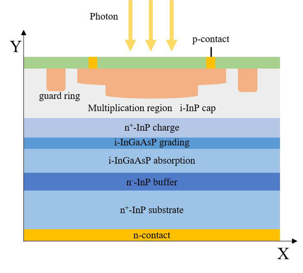
As shown in Fig. 1,a planar front-illuminated InGaAsP/InP SPAD with a SAGCM structure was fabricated based on the previous research. The SAGCM structure was grown on an n-doped InP substrate using a Metal-Organic Chemical Vapor Deposition(MOCVD),which was as follows:InP buffer layer,1.5 μm undoped InGaAsP absorption layer,InGaAsP graded layer,n-doped InP charge layer and undoped InP cap layer. A double Zn-diffusion was performed in the cap layer to create the p-doped region and a floating guard ring,which controls the electric field intensity in the periphery region to be lower than that in the center region of the active area,preventing the premature edge breakdown effect. The sufficient electric field was provided in the multiplier layer to achieve effective collision and ionization,while a lower electric field was maintained in the absorption layer to reduce the tunneling current. During the device fabrication process,the diffusion process was strictly controlled to decrease the deep-level defects in the material [14],and the photosensitive diameter was controlled to 50 μm. For front-illumination devices,the back-side of the chip was gold-plated to serve as an ohmic contact for n-electrode,and the unabsorbed light was reflected back to the absorption layer for secondary absorption,thereby further enhancing the detection efficiency.
Figure 1.Cross-sectional schematic of the InGaAsP/InP APD
Here,the Sentaurus-TCAD,a commercial software,was used to simulate the performance of InGaAsP/InP SPAD. A 2D electric field distribution at a bias voltage of 2 V is shown in Fig. 2,where it can be seen that the electric field at the edge of the active region was effectively controlled. Additionally,the electric field in the InGaAsP absorber remained below 1e5 V/cm,while the electric field in the multiplication region approached 5e5 V/cm,ensuring a high avalanche probability in the InP multiplication layer as well as a low tunneling dark current in the InGaAsP absorption layer.
Figure 2.2D electric field distribution at 2 V over bias
For a SPAD,the PDE can be expressed as the product of three probabilities,as shown in the formula(1):
,
Here,represents the quantum efficiency of carriers caused by incident photons at the InGaAsP absorption layer;represents the probability of carrier injection into the InP multiplication region;represents the avalanche probability in the multiplication layer. For an APD with an absorption coefficient of 1.37×104 cm-1 at 300 K,the is 87.2%. Assumingwas 100%,the theoretical calculation results are presented in Fig. 3. At an overbias voltage of 6 V,can reach nearly 95%,resulting in a PDE of 82.55%. Therefore,through improving the material quality and optimizing the electric field distribution,a PDE of over 70% could be achieved. Subsequently,the performance was characterized experimentally.
The sample and a three-stage thermoelectric cooler(TEC)were integrated together inside a To-66 tube shell,as shown in Fig. 4,allowing the chip to operate at temperatures as low as -50 ℃. A 62.5 μm/125 μm multimode fiber was coupled the incident light through a lens to the SPAD. At different operating temperatures,the device’s current-voltage(I-V)characteristic curves are displayed in Fig. 5.
Figure 4.Physical appearance of an InGaAsP/InP SPAD
A gated-mode single-photon detection system,as shown in Fig. 6,was employed to characterize the performance of the SPAD. Two synchronizing signals were generated from a signal generator(SG):one was a pulse signal to the SPAD with a frequency of 1 MHz,a pulse width of 4 ns,and an amplitude of 5 V;the other was a synchronous trigger signal for the laser with a frequency of 100 kHz. The laser had a peak wavelength of 1.06 μm,a pulse width of 100 ps,and an average power of 0.1 photon per pulse. The light was directly coupled to the SPAD via a multimode fiber. Finally,a Time-Correlated Single Photon Counter(TCSPC)was used to record the output signal.
Figure 6.Schematic diagram of gated-mode single-photon detection system
At an operating temperature of 293 K,the PDE was varied by adjusting the bias voltage of the SPAD. The corresponding DCRs and after-pulse probabilities(APPs)for different PDEs were measured,and then,it is presented in Fig. 7. As the PDE increased,so did the DCR and APP. When the PDE reached 70%,the DCR was only 14.93 kHz with an APP of 0.89%. If the PDE was less than 50%,the DCR remained below 5 kHz. Furthermore,for a PDE of 20%,the DCR reduced to mere 0.4 kHz.
Figure 7.DCRs and APPs corresponding to different PDEs at 293 K
DCR refers to the count when there was no photons incident,mainly derived from the thermal noise and tunneling noise of the device. This parameter can be calculated using formula(2). During the laser shutdown period,the total count within a unit time is recorded as .represents the number of gate pulses within a unit time,and is the pulse width of a gate pulse.
,
The SPAD not only exhibited excellent performance at room temperature but also performed well at low temperatures. As shown in Fig. 8,at 223 K,the DCR can be as low as 0.15 kHz for 70% PDE. When the PDE was less than 30%,the increase rate of the DCR was especially low. Although DCR increased with the temperature,these values remained small due to the relatively low defects and the effective electric field regulation.
Figure 8.The DCR versus temperature at different PDEs
In order to further analyze the origin of the DCR,the activation energy(Ea)was extracted,which can quantitatively describe the composition of the device’s dark current. As shown in Fig. 9,the value was acquired by fitting versus whereis the temperature andis the Boltzmann constant. The results of Ea under various PDEs are shown in Fig. 10. As the PDE increased,the activation energy of the device remained around 0.46 eV with little variation.
An InGaAsP/InP SPAD operated in Geiger-mode with a high reverse bias voltage has a dark current consisting of several components,including the generation-recombination(G-R)current the band-to-band(BTB)tunneling current and the trap-assisted tunneling(TAT)current which can be defined by the following equations [15-16]:
,ħħ,,
Whereis the electron charge,is the intrinsic carrier concentration,is the junction area,is the depletion region width depended on voltage,is the carrier lifetime,is the applied bias voltage,is the effective mass,is the maximum electric field in the junction,ħis the reduced Planck’s constant,is the band-gap energy,is the trap barrier matrix,is the defect concentration,is the built-in field potential,andis the trap energy level.
Here,the G-R current has a strong temperature dependence,including the Shockley-Read-Hall(SRH)dark current associated with deep-level defects and the valence to conduction G-R current. The tunneling current comprises of both BTB and TAT currents,which correlate with the temperature weakly and are in direct proportion to the square of the electric field. The former is due to direct tunneling from the valance band to the conduction band,influenced by relatively high reverse bias voltage in narrow band gap semiconductors and can be reduced by adjusting the thickness of the multiplication layer. The latter originates from the tunneling of electrons via trap levels to the conduction band,influenced by defects in the device. Thus,Ea has been maintained at fixed value,indicating that:(1)As the PDE increases,the tunneling current should rapidly increase with the electric field,resulting a decrease of Ea. However,in this case,Ea remained almost unchanged,indicating that the tunneling current is very small compared to the G-R current,suggesting that there are few defects in the multiplication region.(2)The G-R current accounts for a larger proportion in the dark current. Considering that a portion of it is induced by the valence to conduction generation current while the other part is limited by the deep-level defects,the fixed activation energy close to half of the bandgap energy of InGaAsP indicates that the deep-level defects induced G-R current is dominant. The G-R current varies little with above the value of several kBT/q,ensuring the probability of good single photon performance at room temperature.
When an avalanche occurs,some carriers may be captured by the defects in the material. When the next gate pulse arrives,these captured carriers can cause new avalanches,leading to false signals known as the after-pulse effect. During testing,we set the gate pulse frequency to 1 MHz and the laser frequency to 100 kHz,so for every 10 electrical pulses,only one electrical pulse contains an optical signal. By comparing the counts of the specific electrical pulse containing optical signal and the remaining 9 electrical pulses,the APP was calculated using formula(6). When the laser is turned on,the total count within a unit time is recorded as ,and the count within a gate pulse is. During the laser shutdown period,the total count within a unit time is recorded as .
,
Fig. 11 displays the APP at different temperatures and PDEs. It can be found that the maximum APP was only 0.89%,indicating the presence of few defects in the multiplication region of the SPAD. At the same time,the low APP at high PDE indicates that the error counts caused by the after-pulse effect can be negligible,meaning the high PDE of 70% was real and effective. The low number of dark carriers at low temperatures resulted in a lower probability of defect capture. As the temperature increased,the dark count increased,and the probability of defect capture increased. Therefore,the after-pulse effect raised to some extent with increasing temperature.
Figure 11.APPs versus temperatures at different PDEs
To further characterize the device’s performance,it was also operated in active quenching mode with a dead time of 200 ns,and the results are shown in Fig. 12 and Fig. 13. The laser synchronous trigger frequency was 1 MHz,with an average power of 0.1 photon per pulse. In active quenching mode,the dead time is a critical factor that affects the maximum achievable count rate of the device. To compress the dead time to 200 ns,it is generally necessary to sacrifice the carriers multiplication to suppress the after-pulse effect. Therefore,even at -50 ℃,the PDE could only reach 23.64%,and the DCR was 3.44 kHz. As the temperature increased,the DCR will increase,leading to a further reduction in the achievable PDE. Finally,at room temperature,the PDE was only 12.49%,with a DCR of 72.29 kHz.
Figure 12.PDEs at different temperatures under the active quenching mode
A planar front-illuminated InGaAsP/InP SPAD was presented in this paper. Through electric field regulation,the SPAD’s electric field was mainly concentrated in the center of the multiplication region. Analysis of the activation energy indicated that the main factor affecting the device's DCR was the thermally excited generation-recombination current,and the low number of deep-level defects in the device ensured excellent performance. In gated-mode operation,the InGaAsP/InP SPAD achieved a high PDE of 70% at 293 K,with a low DCR of only 14.93 kHz and an APP of 0.89%. The outstanding performance at room temperature expands the potential applications of the InGaAsP/InP SPADs.
 AI Video Guide
  AI Picture Guide
 AI One Sentence