
Zongtao Li, Kai Cao, Jiasheng Li, Yong Tang, Xinrui Ding, Binhai Yu. Review of blue perovskite light emitting diodes with optimization strategies for perovskite film and device structure[J]. Opto-Electronic Advances, 2021, 4(2): 200019-1
- Opto-Electronic Advances
- Vol. 4, Issue 2, 200019-1 (2021)
Abstract
Introduction
Recently, metal halide perovskites have drawn considerable attention for their distinguished advantages, including high charge carrier mobility
Since Tan et al. reported the first room-temperature EL PeLEDs
Another way to optimize the EL performance of green and red PeLEDs is to finely design the device structure. For example, Wang et al. selected the polyethyleneimine (PEI)-modified low work function metal oxide ZnO and high hole mobility polymer (poly [(9,9-dioctylfluorenyl-2,7-diyl)-co-(4,40-(N-(4-sec-butylphenyl diphenylamine)]) (TFB) as the electron transport layer (ETL) and hole transport layer (HTL) materials, respectively and fabricated high luminance red PeLEDs with a novel inversed device structure
In addition to red and green PeLEDs, the fabrication of blue PeLEDs is also a key factor in the fields of lighting and display. To obtain white PeLEDs, light with two or more different colors must be mixed
In this review, we categorize the recent progress of blue PeLEDs in terms of composition of perovskite films and summarize the main challenges and corresponding optimization strategies. Next, we review the novel strategies for the design of the device structure of blue PeLEDs from the perspective of transport layers and the interface of the EML and CTLs. Finally, future directions for blue PeLEDs are analyzed.
Challenges and optimization strategies for perovskite films of blue PeLEDs
Pure 3D perovskites
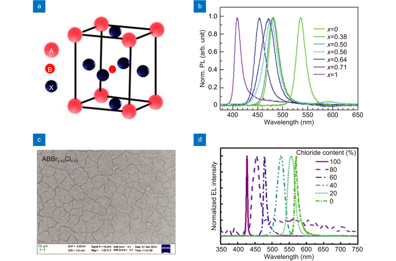
Three-dimensional (3D) metal halide perovskites are defined by a chemical formula of ABX3, where the A site refers to the monovalent cations, including the organic cations (MA+, FA+) and inorganic cation (Cs+, Rb+), the B site refers to the divalent cations (Pb2+, Sn2+, Ti2+), and the C site refers to the halide ions (I-, Br-, Cl-). A divalent cation, such as Pb2+, can form an ionic bond with the halide ions and form a periodically aligned octahedron structure [PbX6]-, while a monovalent cation can insert into the intervals between [PbX6]- to reach charge conversation and stabilize the crystal structure (Fig. 1(a)).
![]()
Figure 1.
As for 3D perovskites, the CBM energy level is dependent on the p-orbital of the divalent cation, while the VBM energy level is related to the p-orbital of the halide ions. By increasing the ratio of Cl-, the VBM is down-shifted and the bandgap of perovskite can be enlarged
Morphology optimization strategies
In general, dense and uniform perovskite films with few pinholes are beneficial for the elimination of leakage current, which is essential for the enhancement of EQE and reduction of Joule heat. The morphology can be modified by adjusting the molar ratio of perovskite precursors. Wang et al. fabricated dense and uniform polycrystalline MAPb(Br1−xClx)3 films by increasing the molar ratio of MA+ and decreasing the whole concentration of the precursors. The results suggested that the small perovskite grain size as well as the thin perovskite film thickness are crucial for facilitating the radiative recombination rate. Optimized sky-blue (490 nm) PeLEDs showed a maximum luminance of 154 cd/m2 at 4.1 V
All inorganic metal halide perovskites show superior thermal stability compared with their organic counterparts. Wang et al. doped RbBr and RbCl into the CsPbBr3 precursor solution. By adjusting the ratios of Rb+, Br- and Cl-, they built up sky-blue (492 nm), blue (473 nm) and deep-blue (468 nm) PeLEDs. The radius of Rb+ (161 pm) is smaller than that of Cs+ (174 pm) and the incorporation of Rb+ into the CsPbBr3 enlarges the bandgap of perovskites and causes the blue shift of the emission spectra. The film morphology can also be improved by Rb+ incorporation to modulate the nucleation process. The lower solubility of RbX compared with CsX facilitated the initial precipitation of RbX small crystals, which can act as nucleation cores that increase the number of perovskites and decrease the size of as-formed perovskite grains. The coverage of perovskite films increased from 80% to 99% (Fig. 2(a)). The maximum luminances of sky-blue (492 nm) and blue (473 nm) PeLEDs are 244 cd/m2 and 112 cd/m2, respectively. It is worth mentioning that all RbX-incorporated blue PeLEDs exhibit great EL spectral stability, indicating improved structural stability by RbX incorporation. However, the low PLQY (<0.25%) of Rb-Cs alloy perovskite films limits the further improvement of device efficiency (EQE = 0.062% for blue device), which originates from the increased number of grain boundaries that facilitate the nonradiative recombination rate
![]()
Figure 2.
Defect passivation strategies
Although 3D perovskites have exhibited outstanding conductivity, the low PLQY of pure 3D perovskite films caused by the large number of defect sites inside the grains or at the grains boundaries limits the further improvement of device performance. As mentioned above, Rb+-incorporated pure 3D perovskite films show good film morphology but low PLQY due to the high defect density at grain boundaries. To diminish the defect density and improve the PLQY of Rb+-incorporated perovskite films, Yuan et al. proposed a cocktail cation strategy that incorporates four kinds of monovalent cation, Rb+, Fa+, PEA+, and K+, into CsPbBrxCl3-x perovskites and fabricated sky-blue (484 nm) PeLEDs with an improved EQE of 2.01%. Also, the EL spectra remain stable under different bias voltage, indicating a suppressed halogen migration (Fig. 2(b)). The results showed that Rb+ can play an important role in optimizing the film morphology with increased coverage and decreased surface roughness, while K+ and PEA+ can form a passivation layer outside the grains to suppress the nonradiative recombination, leading to an improved PLQY from 0.94% to 17.1%
Therefore, even though 3D perovskite films exhibited some excellent properties such as solution processability and high conductivity, the large number of defect sites as well as the low exciton bonding energy limits further improvement of the PLQY. Besides, the low solubility of PbCl2 limits the degree of hypsochromic shift of the emission spectra. Based on the current research findings, several strategies should be considered for the further optimization of pure 3D perovskites films: 1) Adopting the A site mixing strategy. It has been demonstrated that mixing A site cations can promote the device performance through improving the film morphology and slowing down the halogen mobility. Based on that, the category and the molar ratio of the selected A site cations should be thoroughly considered. 2) Adoping O atoms contained passivation agents. Except for the commonly used amino-functionalized moieties, O atoms contained passivation agents should also be exploited as the inductive effect caused by O atoms has been proved to be beneficial for improving the passivation efficiency. 3) Adopting Cl-contained doping agents. In order to fabricate stable blue and deep-blue 3D PeLEDs, the Cl concentration in the final 3D perovskite films should be raised. Cl-contained agents such as the organic chlorines can be suitable for increasing the molar ratio of Cl through either doping into the precursor solution or post treatment.
Colloidal perovskite quantum dots (PQDs)
Compared with pure 3D perovskites, colloidal perovskite quantum dots (PQDs) possess advantages including high EB (~40 meV), low defect density, and high environmental stability. All inorganic CsPbX3 QDs show better water and thermal stability compared with their organic counterparts, which are the most widely researched PQDs. As the PLQYs of PQDs dispersed in solution have reached up to ~100%, PeLEDs with PQDs as the emissive layer may have higher EQE theoretically. Similar with pure 3D blue perovskites, most blue PQDs are synthesized by a mixed halides strategy due to the low solubility of PbCl2 in polar solvent. In 2015, Song et al. synthesized all inorganic blue CsPbBrxCl3-x QDs by the hot-injection method. The as-synthesized PQDs emitted at 455 nm with PLQY up to 60% in dispersion. Moreover, PQD-based blue PeLEDs were fabricated for the first time with a maximum luminance of 742 cd/m2 and EQE of 0.07%
Conductivity optimization strategies
To improve the conductivity of PQD films, excess amounts of insulated ligands should be diminished without lowering the PLQY of PQDs. Pan et al. adopted a ligand exchange strategy to improve the conductivity of PQD films. The halide ion-pair ligand of di-dodecyl dimethyl ammonium bromide (DDAB) was added to the dispersion to thoroughly substitute the long-chain oleic acid ligands at the surface of PQDs. Such a ligand exchange process can be triggered because of the stronger affinity between Br- and the positive site (Cs+ and Pb2+) compared with the oleic group as well as the stronger affinity of DDA+ with the negative sites (Br-) on the PQD surface. The shorter chain length of DDA+ successfully improved the conductivity of PQD films. By substituting the DDAB with the mixed halide-ion-pair ligand di-dodecyl dimethyl ammonium bromide chloride (DDABrCl), sky-blue (490 nm) PQD-based PeLEDs were fabricated with maximum EQE of 1.9%
Morphology optimization strategies
The poor morphology of PQD films can be explained from two aspects. On the one hand, the long-chain ligands, such as oleic acid (OA) and oleylamine (OAm), show poor affinity to the PQD surface, which leads to severe ligand loss during the purification and film formation process. Such a ligand loss phenomenon leads to poor coverage of PQD films due to the weakened dispersibility of PQDs, which can cause severe agglomeration. This ligand loss phenomenon can be even worse in blue-emitting PQDs due to the poor affinity of ligands with Cl-. On the other hand, the concentration of PQDs in dispersion is too low to form a dense and uniform perovskite film, so the leakage current of PQD-based PeLEDs can be further increased. To optimize the morphology of PQD films, Li et al. applied a vapor-based crosslinking strategy that treated PQD films with trimethylaluminum (TMA) vapor
In addition to the modification of ligand affinity, some novel film formation technologies can also be helpful for the improvement of blue PQD film morphology. Deng et al. noted that the main reason for the high surface roughness and excessive pinholes of PQD films originates from the relatively low concentration of PQDs in dispersion (~0.5 mg/ml). By applying a dip-coating method, dense and uniform blue PQD films were formed due to the optimized film formation process. High luminance (2473 ± 105 cd/m2) deep-blue (445 nm) PeLEDs were fabricated with an average EQE of 1.18% thanks to the improved film morphology
Spectra tuning strategies
The traditional strategies for spectra tuning include adjusting the ratio of halides in precursor solution and the halogen exchange. Shin et al. applied a ligand-mediated post-treatment strategy by using both DDAB and DDAC as the ligands to synthesize blue PQDs. Different ratios of the DDAB and DDAC ligands were added to the dispersion to control the degree of halogen exchange by adjusting the concentration of Cl-. Blue PeLED based on this DDAB/DDAC modified PQDs was fabricated (Fig. 3(a)), and the EL spectra could be adjusted from 460 nm to 480 nm
![]()
Figure 3.
Defect passivation strategies
Previous research in the field of PQD synthesis has shown that the incorporation of metal ions, such as K+, Rb+, Cd+, Ni+, Mn2+, Ca2+, Mg2+, La3+, Al3+, and Y3+, into the precursor solution can diminish the generation of defect sites like halogen vacancies at the surface of PQDs by forming a passivation layer outside or hindering the generation of structural defects inside the PQDs by partially doping into the crystal lattice
![]()
Figure 4.
As discussed above, the PLQY of PQDs in dispersion has reached 100% across the entire blue emission spectra region. However, the EQE of PQD-based devices is much lower than the PLQY in dispersion, which can be referred to the poor morphology and conductivity of PQDs films. To improve the quality of PQDs films, strategies are raised up in the following aspects: 1) Eliminating the long-chain ligands like OA and OAm during the preparation of PQDs. Short-chain organic ligands or metal ions can act as the capping agents to substitute the insulated long-chain ligands, which can not only facilitate the charge carriers injection into the PQDs, but also improve the ligand loss phenomenon since the electrostatic force between the short chain ligands/metal ions and the PQDs is strengthen. 2) Reducing the diameter of PQDs. PQDs with small diameter tends to form a compact alignment during the films formation process, which is beneficial for not only the charge transport among PQDs but also the coverage of PQDs films. As the ligand substitution has been proved to be an effective method to decrease the diameter of PQDs, the category of the short chain ligands or metal ions selected for the substitution and the reaction condition should be thoroughly investigated.
Colloidal perovskite nanoplatelets (PNLs)
Besides the Br/Cl mixing strategy, the bandgap of perovskites can also be enlarged by minimizing the grain size so it is smaller than the exciton Bohr radius to trigger the quantum confinement effect. Theoretical calculation exhibited that the exciton Bohr radii of FAPbBr3 and CsPbBr3 are 3.5 nm and 7 nm
In 2015, Bekenstein et al. synthesized colloidal CsPb(Br/Cl)3 PNLs for the first time by a similar hot-injection synthesis procedure as that for PQDs, with the reaction temperature decreased from 130 ℃ to 90 ℃. Ethyl acetate and methyl-ethyl ketone were selected to purify the PNLs without causing damage to the crystal structure. Colloidal PNLs with lateral sizes of n=1 to 5 (where n refers to the number of [PbX6]4- octahedron layers) were synthesized simultaneously when the reaction temperature was 130 ℃
Grain size modification strategies
The categories, concentrations of precursors, and reaction conditions greatly influence the grain size of colloidal PNLs and the morphology of PNL films, which can further influence device performance. In 2016, Kumar et al. synthesized colloidal CsPbBr3 PNLs with exact layer thicknesses of n=1 (deep-blue), n=3 (blue), and n=5 (sky-blue) through precise control of the concentrations and molar ratios of OA, OAm, and MA+. A room-temperature EL PeLED based on colloidal CsPbBr3 nanoplatelets as the emissive layer was fabricated for the first time (Fig. 5(a)). However, the maximum luminance and EQE degraded as the layers of PNLs decreased, which originated from the severe loss of ligands during the film formation process
![]()
Figure 5.
Defect passivation strategies
The defect passivation of colloidal PNLs mainly refers to the passivation of halogen vacancies defects at the surface of colloidal PNLs. Bohn et al. adopted the post-treatment strategy of blending PbBr2, OA, and OAm in solution with a colloidal PNL dispersion with layer thicknesses of n=2 and 3. The increased concentration of Br- in dispersion can effectively repair the Br vacancies at the surface of colloidal PNLs, with PLQY in dispersion increasing from 7% and 9% to 49% and 60% for colloidal PNLs with layer thicknesses of n=2 and 3, respectively. Deep-blue (464 nm) PeLEDs with colloidal PNLs (n=3) as the emissive layer were fabricated with increased color purity (full width at half maximum (FWHM)<20 nm) (Fig. 5(c))
Colloidal PNLs are regarded as a promising candidate for PeLEDs with emission spectra in deep blue region. However, the largely existed defects at the surface of PNLs caused by the large surface/volume ratio facilitated the nonradiative recombination process. Those defects at the surface of PNLs can also strength the ligand loss phenomenon, which is harmful to the size control of PNLs due to the agglomeration of PNLs that can facilitate the unwanted Ostwald ripening process. Even though the post-treatment as well as in-situ passivation strategies can heal the defect sites at the surface of colloidal PNLs and increase the PLQY to near 100% in dispersion, Ostwald ripening process can happen during the preparation of PNLs films and device operation process so that degrading the device performance. To improve the device performance, surface defects as well as the Ostwald ripening process should be eliminated, which can be realized as the following aspects: 1) Eliminating the long-chain ligands like OA and OAm during the preparation of PNLs. This is the same strategy provided for PeLEDs based on PQDs films, since the short chain or metal ions can form a stronger affinity to the surface of PNLs, hindering the formation of surface defects. 2) Optimizing the film formation process. As the Ostwald ripening process can happen during the spin-coating and the annealing process, novel film formation strategy should be exploited to weaken the unwanted regrowth of PNLs.
Quasi-2D perovskites
Quasi-2D perovskites, also called Ruddlesden-Popper perovskites, are defined as perovskites with structure formula L2An−1BnX3n+1. The L site usually refers to bulk organic ammonium cations (abbreviated as bulk cations), the A site refers to the monovalent cations, the B site refers to the divalent cations, and the X site refers to halogens. The bulk cations can act as ligands in the colloidal synthesized PQDs and PNLs, which can limit the growth of perovskite grains. Quasi-2D perovskite films are composed of low-dimensional perovskites with limited [PbX6]4- octahedron layers (n=1, 2, 3, ···, where the definition of n is analogous to that for colloidal PNLs) and high-dimensional perovskites (n=∞ for 3D perovskites), which are formed simultaneously during the film formation process. This multi-phase structure can act as an energy ladder to promote energy transfer between the different phases. When applying quasi-2D perovskites as the emissive layers, the electron-hole pairs form in the lowest n phases at first and then go through an energy funneling process, finally being collected in the highest n phases. The high carrier concentration in the final perovskite emitting phases is beneficial for the radiative recombination process. Blue-emitting quasi-2D perovskites can be realized by adjusting the bandgap of the highest n phases or lowering the dimension of the highest n phases to trigger the quantum confinement effect.
It can be said that quasi-2D perovskites form a theoretical bridge between pure 3D and PNLs perovskites. Compared with pure 3D perovskites, quasi-2D perovskites exhibited an increased EB due to the restricted grain size that can trigger the quantum confinement effect. Furthermore, the defect densities as well as water/oxygen stability are well-modified compared with those of 3D perovskites thanks to the passivation and protection effects of the bulk cations. Compared with colloidal PQDs and PNLs, quasi-2D perovskite films can be formed directly from a precursor solution without a purification process, so the ligands loss phenomenon can be fully eliminated during the film formation process. Moreover, the carbon chain length of commonly used bulk cations in quasi-2D perovskites is much shorter than that in long-chain ligands, such as OA and OAm, so the conductivity of quasi-2D perovskite films can be much better compared with that of PQD or PNL films.
In early studies, researchers aimed to find suitable bulk cations to fabricate blue-emitting quasi-2D PeLEDs. Hu et al. doped BABr into the precursor and fabricated RGB quasi-2D PeLEDs by the mixed halides strategy. However, the luminance and efficiency of sky-blue PeLEDs are considerably lower those of red and green ones because of the considerably high leakage current and poor charge injection into perovskite films
Previous studies have confirmed the significant potential of quasi-2D perovskites for the fabrication of blue-emitting PeLEDs. However, the following two main problems must be resolved for further improvement of device performance. One of the problems is the modulation of the phase distribution. As quasi-2D perovskite films are composed of multiple phases, the energy funneling process limits deep-blue emission because the excitons or free charges will finally be concentrated and radiatively recombined in the phases with the narrowest bandgap (the highest n phases). While adding excess amounts of bulk cations can facilitate the generation of low-n phases and more effectively passivate surface defects, the insulating property of bulk cations can degrade the charge transfer efficiency between different phases, such that the color purity of quasi-2D blue PeLEDs is degraded with multiple emission peaks. In fact, the PLQY, conductivity, and color purity of quasi-2D perovskite films cannot be optimized simultaneously by simply adjusting the concentration of the bulk cations; therefore, strategies for the precise modulation of phase distribution should be exploited. The other problem is the stability of the EL spectra. Although most bulk cations are hydroscopic which can effectively improve the water stability of quasi-2D perovskites. Exposure to UV light, electric field, and Joule heat produced during the operating process can destabilize the quasi-2D perovskites and lead to the phase segregation phenomenon, which can cause the red-shift of emission spectra, decreasing the device operating lifetime. In this section, strategies for phase modulation as well as the improvement of spectral stability are reviewed.
Phase modulation strategies
Phase modulation strategies are performed to obtain blue-emitting quasi-2D perovskite films with narrow emission spectra, short emission wavelength, and high PLQY. The primary task for the phase modulation is to obtain blue-emitting perovskite films, which can be realized through either enlarging the bandgap of 3D phases in quasi-2D perovskite films or narrowing the phase distribution with only low-n phases to trigger the quantum confinement effect. Generally, the 3D phases have the narrowest bandgap in quasi-2D films, which can be effectively enlarged by the mixed Br/Cl strategy. Moreover, when applying the mixed Br/Cl strategy, the concentration of bulk cations can be adjusted to a suitable range without reducing the conductivity. Vashishtha et al. prepared all inorganic quasi-2D blue PeLEDs for the first time by simultaneously adjusting the concentration of BA cations as well as the ratio of Br/Cl in precursor solutions. The EL spectra exhibited a wide tuning range with EL peak wavelength varied from 465 nm to 500 nm (Fig. 6(a)). The concentration of BA cations was also well controlled to achieve PeLEDs with pure emission. The FWHM of the EL spectra were 22 nm and 23 nm for the sky-blue (488 nm) and deep-blue (465 nm) PeLEDs, respectively. The EL performance of the sky-blue and deep-blue PeLEDs was improved, with maximum luminances of 3340 cd/m2 and 962 cd/m2 and EQEs of 6.2% and 2.4%, respectively
![]()
Figure 6.
Besides enlarging the bandgap of 3D phases in quasi-2D perovskite films, the other way to obtain blue-emitting quasi-2D-based PeLEDs is to narrow the phase distribution of the obtained quasi-2D perovskite films with low-n phases to trigger the quantum confinement effect. The dimension of quasi-2D phases can be restricted with only low-n phases (n≤4) existing by precisely controlling the crystallization rate. Liu et al. optimized the crystallization rate by adding large amounts of PBA cations and using ethyl acetate as an anti-solvent to wash away excess PBA cation. The composition of the as-prepared quasi-2D perovskite films was unique with CsxFa1-xPbBr3 nanocrystals (NCs) embedded within the layered perovskites. The radius of CsxFa1-xPbBr3 NCs can be adjusted from 5.3 Å to 6.7 Å by decreasing the molar ratio of PBA cations, which leads to an adjustable emission spectra from 474 nm to 494 nm. The obtained films showed a high PLQY of 60% with a low stimulation power of 0.24 mW/cm2, indicating nearly no energy loss during the energy transfer process. The as-prepared PeLEDs showed a maximum luminance and EQE of 700 cd/m2 and 9.5%, respectively
Several novel film formation strategies have been applied to fabricate quasi-2D perovskite films with pure phase, which is beneficial for the precise control of the emission spectra. Liang et al. fabricated pure 2D PEA2PbBr4 perovskites using DMF vapor annealing methods. Deep-blue (410 nm) PeLEDs based on PEA2PbBr4 nanoplates as the emissive layer were fabricated for the first time. The obtained PEA2PbBr4 nanoplates fabricated by the DMF vapor annealing methods showed enlarged lateral length on micrometer size, which could reduce the defect density and enhance the PLQY due to the diminished grain boundaries. However, the discontinuous film morphology caused large leakage current, with the optimal device exhibiting a low EQE of 0.02%
Spectra-stabilizing strategies
Spectral stability refers to the ability of the emission spectra to remain stable against harsh environmental conditions, such as UV exposure, water/oxygen exposure, high temperature, and high operating voltage. Due to the large difference of the electronegativity between Br- and Cl-, the Br/Cl mixed PeLEDs showed severe phase separation during the device operating process, which caused red-shift of the EL spectra. For example, the PeLEDs fabricated by Vashishtha
Several strategies have been provided to improve the EL spectral stability of PeLEDs based on Br/Cl mixed phases. Tan et al. found that the red-shift of EL spectra during operation is reversible, indicating that the phase separation process caused by the electric fields is recoverable. When the applied voltage was changed from direct voltage to square-wave alternating voltage (SWAV), this spectrum recovering process could be sped up. By optimizing the voltage bias (6 V for forward direction and -4 V for reverse direction), duty ratio (0.25), and frequency (50 Hz) of the SWAV, the EL peak position could remain unchanged at 466 nm for 12 h, which is one of the blue PeLEDs with the most stable EL spectra
![]()
Figure 7.
Usually, pure Br-based PeLEDs show better spectral stability due to the relieved phase segregation effect. However, red-shift of emission spectra can still occur for pure Br-based PeLEDs due to the regrowth of quasi-2D perovskites through the Ostwald ripening process. Leung et al. adopted DFT calculations and found that compared with sole BA cation-based quasi-2D perovskites, quasi-2D perovskites with BA/PEA mixing showed better thermal stability due to minimized crystalline strain relaxation during the heating process. They also observed that the EL spectra of the device based on sole BA cations was red-shifted compared with the PL spectra after the thermal evaporation process, while the EL peak position of the device based on PEA/BA mixing remained stable at 456 nm. The temperature of perovskite films can rise up to 95 ℃ during the thermal evaporation process, which leads to the regrowth of quasi-2D perovskites through the Ostwald ripening process, causing red-shift of the EL spectra
Quasi-2D perovskite films consist of perovskite phases with multi-dimensions, which combines the advantages of both pure 3D and colloidal perovskites. Quasi-2D blue PeLEDs have achieved continuous breakthrough in optimizing device performance and stability. However, there is still much room for the further improvement, with research directions in the following aspects: 1) Optimizing the phase distribution. The category and molar ratio of the bulk cations play a key role in modifying the phases distribution. Bulk cations with phosphonate radical are the hotspot now, which should be thoroughly investigated. 2) Avoiding the Efficiency roll-off issue. The mechanism and strategies focus on this efficiency roll-off issue at high current density is rarely discussed in optimizing blue PeLEDs. The Auger recombination can be a possible mechanism for the efficiency roll-off issue at high current density, other reasonable explanations as well as optimization strategies should be provided to further improve the device performance of quasi-2D blue PeLEDs.
Challenges and optimization strategies for device structures of blue PeLEDs
The most commonly used device structure of PeLEDs is the “sandwich-like” structure with the CTLs inserted between the electrodes and the perovskite film. The HTL/ETL materials can prevent the leakage current caused by direct metal contact and provide additional energy levels to reduce the large energy offset between the electrode and the perovskite film, which facilitates charge injection. Compared with those of red and green PeLEDs, the device structure design of blue PeLEDs is more complicated. This is because the energy offset between the electrode and blue perovskites is much larger than those of its red and green counterparts. Such an energy offset severely hinders charge injection, especially hole injection, as the VBM of blue perovskite can be as deep as upto 7.1 eV
Single-layered electron/hole transport optimization strategy
The single-layered electron/hole transport optimization strategy refers to the assembly of CTL materials with suitable energy levels and high charge carrier mobility to substitute for traditional organic counterparts, such as PEDOT:PSS and 2,2',2''-(1,3,5-benzinetriyl)-tris (1-phenyl-1-H-benzimidazole) (TPBi), for the purpose of optimizing the charge transport/injection process and increasing the charge carrier concentration in perovskite films. Yao et al. applied NiOx as the HTL material to fabricated blue PeLEDs for the first time, with an EQE of 0.07%
Multi-layered hole transport optimization strategy
The multiple HTL strategy refers to inserting two or more layers of hole transport materials between the anode and perovskite film. Hoye et al. found that there exists large energy offset (~1.3 eV) between PEDOT:PSS and colloidal PNLs, which not only hindered hole injection rate but also triggered exciton dissociation at the PEDOT:PSS/EML interface. By inserting layers of poly(triarylamine) polymers like TFB or poly(N,N'-bis(4-butylphenyl)-N,N'-bisphenylbenzidine) (POLY-TPD), the energy barrier as well as the nonradiative recombination rate at the interface were minimized. The EQE of as-prepared deep-blue (464 nm) and sky-blue (489 nm) PeLEDs improved two orders of magnitude from 0.007% to 0.3% and 0.004% to 2.4%, respectively
An HTM tri-layer strategy is widely applied in the fabrication of deep-blue PeLEDs with emission peak wavelength less than 470 nm. Kumar et al. fabricated tri-layer HTMs based on the PEDOT:PSS/PVK bilayer structure. Donor materials like 4,4'-bis(N-carbazolyl)-1,1'-biphenyl (CBP) were inserted on top of the PVK layer, and the excitons could transfer and recombine efficiently in the perovskite film through the Förster resonance energy transfer process (FRET). They believed that a large spectral overlap between the absorption spectra of the acceptor materials (perovskites) and the donor emission spectra is a prerequisite for the FRET process, which gives guidance for selecting suitable HTL materials
Interface modification strategy
The interface modification strategy refers to inserting a functional layer between the CTL and emissive layer to improve the device performance. Those functional materials cannot be a CTL solely; however, the charge transport efficiency, perovskite film quality, and nonradiative recombination at the interface can be optimized by the modification of functional materials. Cheng et al. modified ZnO with polyethylenimine ethoxylated (PEIE) to decrease the work function of ZnO. The energy offset between the ZnO and perovskite film was reduced, which is beneficial for electron injection. Sky-blue (490 nm) PeLEDs based on PEIE-modified ZnO substrates showed a low turn-on voltage of 2.9 V
![]()
Figure 8.
An energy diagram of the commonly used ETL/HTL materials is shown in Fig. 9. In short, the key factors for device structure design of blue and deep-blue PeLEDs are as follows: 1) selecting carrier transport materials with matching energy levels against the blue and deep-blue perovskites, 2) increasing the carrier mobility of HTL/ETL materials to facilitate carrier transport, 3) improving the intrinsic stability of HTL/ETL materials, and 4) modifying the interface of CTLs and the perovskite film.
![]()
Figure 9.
| Year | Type | Device Structure | Device performance | |||||
| λ(EL)/FWHM (nm/nm) | EQE (%) | Max lumin (cd/m2) | CE (cd/A) | VT (V) | Ref | |||
| 2016 | 3D Bulk | ITO/PEDOT:PSS/Pero/TPBi/Ca/Al | 490/30 | - | 154 | 0.08 | 4.1 | Ref. |
| 2017 | 3D Bulk | ITO/ZnO/Pero/NPD/MoO3/Al | 475/- | 1.7 | 3567 | 11.31 | 3.2 | Ref. |
| 2018 | 3D Bulk | ITO/AZO:Cs/Pero/CuS-GaSnO/WO3/Ag | 475/19 | 2.58 | 6426 | 15.21 | 3.1 | Ref. |
| 2019 | 3D Bulk | ITO/PEDOT:PSS/Pero/TPBi/LiF/Al | 490/ | 0.58 | 1470 | - | ~4.2 | Ref. |
| 2019 | 3D Bulk | ITO/PEDOT:PSS/Pero/TyPmPb/LiF/Al | 468/20, 492/20 | 0.062, 0.17 | 112,244 | 0.06, 0.32 | 4.4,3.4 | Ref. |
| 2019 | 3D Bulk | ITO/NiOx/Pero/TPBi/LiF/Al | 456/24, 468/23, 480/20 | 0.15, 0.38, 0.05 | 51,121,87 | 0.07, 0.21, 0.04 | 4,3.5,4 | Ref. |
| 2020 | 3D Bulk | ITO/PEDOT:PSS/RbCl/pero/Tmpypb/LiF/Al | 484/12 | 1.66 | 9243 | 2.15 | 2.6 | Ref. |
| 2020 | 3D Bulk | ITO/LiF/pero//LiF/Bphen/Al | 484/22 | 2.01 | 4015 | 2.11 | ~4 | Ref. |
| 2015 | NC | ITO/PEDOT:PSS/PVK/Pero/TPBi/LiF/Al | 455/20 | 0.07 | 742 | 0.14 | 5.1 | Ref. |
| 2016 | NC | ITO/ZnO/Pero/TFB/MoO3/Ag | 480/17 | 0.0074 | 8.7 | - | 5.5 | Ref. |
| 2016 | NC | ITO/PEDOT:PSS/PVK/Pero/TPBi/LiF/Al | 445/30 | 1.18 | 2473 | - | ~7.8 | Ref. |
| 2016 | NC | ITO/PEDOT:PSS/PVK/Pero/TPBi/LiF/Al | 490/19 | 1.9 | 35 | - | 3 | Ref. |
| 2017 | NC | ITO/NiOx/Pero/TPBi/LiF/Al | 470/20 | 0.07 | 350 | 0.18 | ~5 | Ref. |
| 2018 | NC | ITO/PEDOT:PSS/PVK/Pero/TPBi/LiF/Al | 465/15.6 | ~0.2 | ~100 | 0.1 | ~6 | Ref. |
| 2018 | NC | ITO/TFB/PFI/Pero/TPBi/LiF/Al | 469/25 | 0.5 | 111 | - | ~5 | Ref. |
| 2018 | NC | ITO/POLY-TPD/Pero/TPBi/LiF/Al | 466/23, 502/23 | 0.61, 3.6 | 39, 750 | 8.5@502 nm | ~4 | Ref. |
| 2018 | NC | ITO/PEDOT/TFB/PFI/Pero/TPBi/LiF/Al | 466/17.1 | 2.12 | 389 | - | 4 | Ref. |
| 2019 | NC | ITO/PEDOT:PSS/POLY-TPD/CBP/Pero/B3PyMpM/LiF/Al | 463/14 | 1.4 | 318 | - | 2.9 | Ref. |
| 2019 | NC | ITO/PEDOT:PSS/POLY-TPD/Pero/TPBi/LiF/Al | 458/18,469/18, 479/18 | 0.1,0.44,0.86 | 3.87, 11.95, 29.95 | 0.06, 0.28, 0.77 | 4.5,4,3.5 | Ref. |
| 2019 | NC | ITO/PEDOT:PSS/POLY-TPD/PVK/Pero/B3PYMPM/TPBi/LiF/Al | 463/18, 476/18, 490/18 | 1.03, 2.25,3.5 | 193, 678, 2063 | - | 3-3.4 | Ref. |
| 2019 | NC | ITO/PEDOT:PSS/POLY-TPD/Pero/TPBi/LiF/Al | 476/20 | 1.96 | 212.9 | - | 3.2 | Ref. |
| 2020 | NC | ITO/TFB/PFI/Pero/3TPYMP/Liq/Al | 471/17 | 6.2 | 465 | - | - | Ref. |
| 2020 | NC | ITO/PEDOT:PSS/TFB/PFI/Pero/TPBi/LiF/Al | 470/- | 2.4 | 612 | - | 3.2 | Ref. |
| 2020 | NC | ITO/PEDOT:PSS/POLY-TPD/Pero/TPBi/Ca/Ag | 469/18, 479/18, 489/18, 496/18 | 0.65,1,1.8,2.6 | 30,119, 182,603 | 0.47, 0.94, 2.4,4.5 | 3.8,3.2,
| Ref. |
| 2020 | NC | ITO/NiOx/Pero/TPBi/LiF/Al | 445/- | 1.12 | 262.6 | 4.5 | Ref. | |
| 2020 | NC | ITO/PEDOT:PSS/POLY-TPD/Pero/TPBi/LiF/Al | 459/- | 0.3 | 76 | 0.3 | - | Ref. |
| 2020 | NC | ITO/PEDOT:PSS/PTAA/Pero/TPBi/LiF/Al | 479/20 | 12.3 | ~600 | - | 2.8 | Ref. |
| 2020 | NC | ITO/PEDOT:PSS/POLY-TPD/PVKPero/TyPmPB/LiF/Al | 462/19, 465/19, 468/20, 470/21 | 0.77,0.92,1.53,
| 450,518, 620,507 | 4.5, 5.1, 5.4,6.0 | 4.4,4.6,
| Ref. |
| 2020 | NC | ITO/PEDOT:PSS/TFB/OAM-ClPero/TPBi/Liq/Al | 456/16 | 1.1 | 43.2 | - | 5.4 | Ref. |
| 2020 | NC | ITO/PEDOT:PSS/TFB/PFI/Pero/TPBi/LiF/Al | 463/17 | 3.3 | 569 | - | 4 | Ref. |
| 2020 | NC | ITO/PEDOT:PSS/POLY-TPD/PFN-X/Pero/TPBi/LiF/Al | 470/17 | 1.34 | 46.7 | 1.24 | 3 | Ref. |
| 2016 | NPL | ITO/PEDOT:PSS/PVK/Host layer/Pero/TPBi/LiF/Al | 432/25, 456/25, 492/25 | 0.23, 0.0240.004 | 8.5 | - | 3.5 | Ref. |
| 2018 | NPL | ITO/PEDOT:PSS/POLY-TPD/Pero/TPBi/LiF/Al | 480/- | ~0.1 | 25 | - | 4.6 | Ref. |
| 2018 | NPL | ITO/PEDOT:PSS/POLY-TPD/Pero/TPBi/Ca/Ag | 464/20 | 0.057 | 38 | - | 3.6 | Ref. |
| 2018 | NPL | ITO/PEDOT:PSS/POLY-TPD/Pero/TPBi/LiF/Al | 463/12 | 0.124 | 62 | 0.117 | 4.2 | Ref. |
| 2019 | NPL | ITO/PEDOT:PSS/TFB or POLY-TPD/Pero/TPBi/Ca/Ag | 464/16, 489/25 | 0.3,0.55 | 48,40 | 0.3,1.1 | 4 | Ref. |
| 2019 | NPL | ITO/PEDOT:PSS/POLY-TPD/Pero/TPBi/LiF/Al | 464/18, 490/18 | 0.11, 0.87 | 71,186 | - | 4 | Ref. |
| 2019 | NPL | ITO/PEDOT/POLY-TPD/CBP/Pero/TPBi/LiF/Al | 469/- | 1.42 | 41.8 | - | 3 | Ref. |
| 2020 | NPL | ITO/POLY-TPD/MoO3/Pero/TyPmPB/LiF/Al | 439/14 | 0.14 | 9.7 | - | 3.6 | Ref. |
| 2016 | Quasi-2D | ITO/PEDOT:PSS/Pero/TPBi/Ca/Al | 410/14 | 0.038 | - | - | 2.5 | Ref. |
| 2016 | Quasi-2D | ITO/ZnO/PEIE/Pero/TFB/MoOx/Al | 491/broad | 0.015 | 186 | - | 2.9 | Ref. |
| 2016 | Quasi-2D | ITO/PEDOT:PSS/POLY-TPD/QW-Pero/TPBi/LiF/Al | 468/28 | 0.01 | 21 | 0.006 | 5.2 | Ref. |
| 2016 | Quasi-2D | ITO/PEDOT:PSS/Pero/TPBi/Ba/Al | 462/broad,
| 0.06,1.1 | 1.62, 19.25 | 0.07,2.1 | - | Ref. |
| 2017 | Quasi-2D | ITO/PEDOT:PSS/Pero/TypmpB/CsF/Al | 485/broad | 2.6 | 200 | - | 3.4 | Ref. |
| 2018 | Quasi-2D | ITO/PEDOT:PSS/NiOx/PVK/Pero/TPBi/LiF/Al | 490/28 | 1.5 | 2480 | 2.8 | 5 | Ref. |
| 2018 | Quasi-2D | ITO/PEDOT:PSS/PVK/Pero/TPBi/LiF/Al | 465/23, 487/22 | 2.4,6.2 | 962, 3340 | 1 | 5, 4.5 | Ref. |
| 2018 | Quasi-2D | ITO/NiOx/LiF/Pero/TPBi/LiF/Al | 473/24, 481/24,490/24 | 0.16, 0.25, 0.52 | 217, 509, 1446 | - | 3.5 | Ref. |
| 2019 | Quasi-2D | ITO/PEDOT:PSS/Pero/TPBi/LiF/Al | 480/21 | 5.7 | 3780 | 6.2 | 3.2 | Ref. |
| 2020 | Quasi-2D | ITO/PVK:F4-TCNQ/Pero/TPPO/TPBi/LiF/Al | 492/18 | 8.2 | 1687 | 13.1 | ~3.8 | Ref. |
| 2019 | Quasi-2D | ITO/PEDOT:PSS/Pero/Tmpypb/LiF/Al | 475/25 | 1.35 | 100.6 | ~1 | ~3 | Ref. |
| 2019 | Quasi-2D | ITO/PVK/Pero/TPBi/LiF/Al | 474/34,484/34 | 0.002, 0.13 | 4,45 | 0.002, 0.14 | ~3 | Ref. |
| 2019 | Quasi-2D | ITO/PEDOT/PVK:10%TAPC/Pero/TPBi/Ca/Ag | 410/11.6 | 0.31 | 147.6 | 0.19 | 4.2 | Ref. |
| 2019 | Quasi-2D | ITO/NiOx/PSSNa/Pero/TPBi/LiF/Al | 493/25 | 1.45 | 5737 | 2.25 | 3.3 | Ref. |
| 2019 | Quasi-2D | ITO/NiOx/TFB/PVK/Pero/TPBi/LiF/Al | 483/26 | 9.5 | 700 | - | 3.3 | Ref. |
| 2019 | Quasi-2D | ITO/PVK/PFI/Pero/3TPYMB/Liq/Al | 465/21 | 2.6 | 211 | ~1.3 | 3 | Ref. |
| 2019 | Quasi-2D | ITO/PEDOT:PSS/Pero/TPBi/LiF/Al | 468/25 | 0.71 | 122 | 0.78 | 4.5 | Ref. |
| 2019 | Quasi-2D | ITO/PEDOT:PSS or NiOx/Pero/TPBi/LiF/Al | 480/-, 490/-, 499/- | 1.43,2.4,1.58 | 919,2825,7759 | 1.53, 3.67 | 3.5,3.3,
| Ref. |
| 2019 | Quasi-2D | ITO/PVK/Pero/PO-T2T/Liq/Al | 485/23 | 2.62 | 1200 | - | 2.6 | Ref. |
| 2019 | Quasi-2D | ITO/PEDOT:PSS/Pero/TPBi/LiF/Al | 487/- | 11 | 9048 | - | ~3 | Ref. |
| 2019 | Quasi-2D | ITO/NiOx:F6TCNNQ/PVK/Pero/TPBi/Cs2CO3/Al | 456/-, 468/- | 0.0150.026 | - | - | - | Ref. |
| 2020 | Quasi-2D | ITO/PEDOT:PSS/Pero/TPBi/LiF/Al | 450/-, 482/- | 0.7, 1.1 | - | - | - | Ref. |
| 2020 | Quasi-2D | ITO/PEDOT:PSS/Pero/TyPmPB/LiF/Al | 494/- | 2.7 | 465 | 4.3 | 3 | Ref. |
| 2020 | Quasi-2D | ITO/PEDOT:PSS:PFI or POLY-TPD/Pero/TPBi/LiF/Al | 489/18,479/18 | 1.3,5.2 | 5184, 412 | - | ~4 | Ref. |
| 2020 | Quasi-2D | ITO/PEDOT: PSS/Pero/TPBi/Ca/Al | 485/- | 7.84 | 1130 | - | 4.3 | Ref. |
Table 1.
Conclusion
In this paper, the recent achievements of blue PeLEDs were reviewed from two aspects: optimization strategy for blue-emitting perovskite films as well as the design of device structure. For achieving high-quality perovskite films with low defect density, pure emission, and good film morphology, different optimization strategies focusing on either the perovskite precursor or perovskite film formation process have been proposed based on the features of the four kinds of perovskite materials. For achieving blue-emitting PeLEDs with high charge carrier concentration in perovskite films, balanced charge injection rate, and low interface energy loss, the device structure should be well-designed. Here, we present a discussion on the features and future development directions of the four kinds of perovskite materials as well as the design of device structure.
Features and outlook for pure 3D perovskites
Pure 3D perovskites show optimal conductivity, which is beneficial for charge carrier injection into the perovskite film. However, the lowest EB as well as the significant number of defect sites degrade the PLQY of pure 3D perovskite films, which limits the efficiency of PeLEDs based on pure 3D perovskites. Besides, the fabrication of pure 3D perovskite-based PeLEDs in the of deep-blue spectral region (<470 nm) remains a challenge. Due to the poor solubility of PbCl2, most blue-emitting 3D perovskites have mixed halide components, which easily succumb to phase segregation during device operation. The most effective way to improve the stability of pure 3D PeLEDs is mixing A site cations, which should be regarded as a potential development direction for stable pure 3D PeLEDs in deep-blue region.
Features and outlook for colloidal PQDs and PNLs
Compared with pure 3D PeLEDs, colloidal PQDs show better water and oxygen stability due to the existence of long-chain alkyl ligands at the surface of PQDs. These ligands can not only protect the PQDs from water and oxygen but also passivate the defect sites at the surface, especially halogen vacancies. PLQYs of colloidal PQDs have reached almost 100%. By precisely controlling the reactive conditions and concentrations of various precursors, colloidal PNLs can be synthesized with precise thickness. The emission spectra can be tuned from 405 nm to 490 nm by adjusting the layer thickness of colloidal PNLs from n=1 to 5 due to the quantum confinement effect. However, these two kinds of colloidally synthesized perovskites have similar inherent shortcomings. First, the PLQYs of colloidal PQDs or PNLs in films are much lower than that in dispersion. The main reason for this degradation is the severe ligand loss during the purification and film formation processes, especially in PNLs with larger surface/volume ratios. Also, the insulating property of the alkyl chain hinders the charge injection into these colloidal perovskite materials. To improve the PLQY in film state, the ligand loss problem should be solved. Ligands with better affinity should be selected, and other modification strategies, such as post-treatment and in-situ passivation should be applied to enhance the electronic interaction between ligands and perovskites. To improve the conductivity of colloidal perovskite films, ligands with shorter chain lengths should be adopted. The most promising way to promote the conductivity of colloidal perovskite films is to use metal ions as capping ligands. As Na+, K+ and Ca2+ are metal ions that has been applied to modify blue PQDs as capping ligands to fabricate PeLEDs, other metals ions should be exploited.
Features and outlook for Quasi-2D perovskites
Quasi-2D perovskites may be the most promising materials to fabricate high-efficiency blue PeLEDs. By using bulk organic ammonium cations as the ligands, quasi-2D films composed of multi-dimensional phases of perovskite can be achieved in solid film state. The existence of multi-dimensional phases enables quasi-2D perovskites to be a bridge that connects pure 3D perovskites and colloidal 2D PNLs. High conductivity as well as high EB properties can be obtained simultaneously, which is the most promising feature of quasi-2D perovskite films. For the future of quasi-2D blue PeLEDs, the dimension distribution of perovskite films should be optimized to diminish the energy loss during the energy transfer process. Strategies like mixing A site cations, mixing bulk cations, and additives engineering, can be utilized to further promote the efficiency and stability of devices based on quasi-2D perovskites. Some novel film formation methods are also useful in the precise control of the dimension distribution of quasi-2D perovskites, which exhibit potential in fabricating PeLEDs with emission spectra in the ranges of deep-blue and ultraviolet.
Features and outlook for device structure
In addition to perovskite films, the proper design of device structure can also improve the EL performance of blue PeLEDs. The strategies for the optimization of device structure of blue PeLEDs can be summarized in three categories: 1) assembling the carrier transport materials properly, 2) adopting multi-layer HTL materials, and 3) utilizing functional materials to modify the CTL/EML interface. All these strategies aim to improve the device performance from several aspects: 1) Improving the charge carrier concentration in the perovskite film. This can be achieved by either increasing the charge mobility of HTM/ETM or minimizing the energy offset between the CTLs and EML. 2) Diminishing the nonradiative recombination at the interface. Some commonly used HTL materials like PEDOT:PSS and NiOx have features of exciton quenching, which can degrade the EL performance of blue PeLEDs. Strategies such as adopting multiple transport layers and inserting functional materials should be applied to modify these imperfect HTL materials. 3) Improving the morphology of perovskite films. As the morphology of perovskite films is related to the properties of underlying substrates, such as hydrophilicity/hydrophobicity, ionicity, and surface roughness. The chemical reactivity of underlying materials with the perovskite precursor should also be considered as perovskites can suffer a phase transition with reaction of the underlying substrates, which has previously been reported for red and green PeLEDs
References
[1] C Wehrenfennig, GE Eperon, MB Johnston, HJ Snaith, LM Herz. High charge carrier mobilities and lifetimes in organolead trihalide perovskites. Adv Mater, 26, 1584-1589(2014).
[2] SD Stranks, GE Eperon, G Grancini, C Menelaou, MJP Alcocer, et al. Electron-hole diffusion lengths exceeding 1 micrometer in an organometal trihalide perovskite absorber. Science, 342, 341-344(2013).
[3] ZG Xiao, QF Dong, C Bi, YC Shao, YB Yuan, et al. Solvent annealing of perovskite-induced crystal growth for photovoltaic-device efficiency enhancement. Adv Mater, 26, 6503-6509(2014).
[4] SM Peng, SS Wang, DD Zhao, XJ Li, C Liang, et al. Pure bromide-based perovskite nanoplatelets for blue light-emitting diodes. Small Methods, 3, 1900196(2019).
[5] DY Luo, R Su, W Zhang, QH Gong, R Zhu. Minimizing non-radiative recombination losses in perovskite solar cells. Nat Rev Mater, 5, 44-60(2020).
[6] W Tian, HP Zhou, L Li. Hybrid organic-inorganic perovskite photodetectors. Small, 13, 1702107(2017).
[7] SA Veldhuis, PP Boix, N Yantara, MJ Li, TC Sum, et al. Perovskite materials for light-emitting diodes and lasers. Adv Mater, 28, 6804-6834(2016).
[8] F Sahli, J Werner, BA Kamino, M Bräuninger, R Monnard, et al. Fully textured monolithic perovskite/silicon tandem solar cells with 25.2% power conversion efficiency. Nat Mater, 17, 820-826(2018).
[9] CY Kong, CH Lin, CH Lin, TY Li, SWH Chen, et al. Highly efficient and stable white light-emitting diodes using perovskite quantum dot paper. Adv Sci, 6, 1970143(2019).
[10] ZT Li, CJ Song, JS Li, GW Liang, LS Rao, et al. Highly efficient and water-stable lead halide perovskite quantum dots using superhydrophobic aerogel inorganic matrix for white light-emitting diodes. Adv Mater Technol, 5, 1900941(2020).
[11] P Chen, ZY Xiong, XY Wu, M Shao, Y Meng, et al. Nearly 100% efficiency enhancement of CH3NH3PbBr3 perovskite light-emitting diodes by utilizing plasmonic au nanoparticles. J Phys Chem Lett, 8, 3961-3969(2017).
[12] ZT Li, K Cao, JS Li, XW Du, Y Tang, et al. Modification of interface between PEDOT:PSS and perovskite film inserting an ultrathin LiF layer for enhancing efficiency of perovskite light-emitting diodes. Org Electron, 81, 105675(2020).
[13] M Lu, Y Zhang, SX Wang, J Guo, WW Yu, et al. Metal halide perovskite light-emitting devices: promising technology for next-generation displays. Adv Funct Mater, 29, 1902008(2019).
[14] ZK Tan, RS Moghaddam, ML Lai, P Docampo, R Higler, et al. Bright light-emitting diodes based on organometal halide perovskite. Nat Nanotechnol, 9, 687-692(2014).
[15] GR Li, ZK Tan, DW Di, ML Lai, L Jiang, et al. Efficient light-emitting diodes based on nanocrystalline perovskite in a dielectric polymer matrix. Nano Lett, 15, 2640-2644(2015).
[16] JQ Li, SGR Bade, X Shan, ZB Yu. Single-layer light-emitting diodes using organometal halide perovskite/poly(ethylene oxide) composite thin films. Adv Mater, 27, 5196-5202(2015).
[17] MJ Yuan, LN Quan, R Comin, G Walters, R Sabatini, et al. Perovskite energy funnels for efficient light-emitting diodes. Nat Nanotechnol, 11, 872-877(2016).
[18] CX Zhang, DB Kuang, WQ Wu. A review of diverse halide perovskite morphologies for efficient optoelectronic applications. Small Methods, 4, 1900662(2020).
[19] JP Wang, NN Wang, YZ Jin, JJ Si, ZK Tan, et al. Interfacial control toward efficient and low-voltage perovskite light-emitting diodes. Adv Mater, 27, 2311-2316(2015).
[20] YF Shi, W Wu, H Dong, GR Li, K Xi, et al. A strategy for architecture design of crystalline perovskite light-emitting diodes with high performance. Adv Mater, 30, e1800251(2018).
[21] H Cho, SH Jeong, MH Park, YH Kim, C Wolf, et al. Overcoming the electroluminescence efficiency limitations of perovskite light-emitting diodes. Science, 350, 1222-1225(2015).
[22] KB Lin, J Xing, LN Quan, Arquer de, XW Gong, et al. Perovskite light-emitting diodes with external quantum efficiency exceeding 20 per cent. Nature, 562, 245-248(2018).
[23] Y Cao, NN Wang, H Tian, JS Guo, YQ Wei, et al. Perovskite light-emitting diodes based on spontaneously formed submicrometre-scale structures. Nature, 562, 249-253(2018).
[24] WD Xu, Q Hu, S Bai, CX Bao, YF Miao, et al. Rational molecular passivation for high-performance perovskite light-emitting diodes. Nat Photonics, 13, 418-424(2019).
[25] ZT Li, CJ Song, ZY Qiu, JS Li, K Cao, et al. Study on the thermal and optical performance of quantum dot white light-emitting diodes using metal-based inverted packaging structure. IEEE Trans Electron Devices, 66, 3020-3027(2019).
[26] CHA Li, ZC Zhou, P Vashishtha, JE Halpert. The future is blue (LEDs): why chemistry is the key to perovskite displays. Chem Mater, 31, 6003-6032(2019).
[27] XJ Zhou, PF Tian, CW Sher, J Wu, HZ Liu, et al. Growth, transfer printing and colour conversion techniques towards full-colour micro-LED display. Prog Quantum Electron, 71, 100263(2020).
[28] ZJ Liu, CH Lin, BR Hyun, CW Sher, ZJ Lv, et al. Micro-light-emitting diodes with quantum dots in display technology. Light Sci Appl, 9, 83(2020).
[29] JS Li, Y Tang, ZT Li, XR Ding, BH Yu, et al. Largely enhancing luminous efficacy, color-conversion efficiency, and stability for quantum-dot white LEDs using the two-dimensional hexagonal pore structure of sba-15 mesoporous particles. ACS Appl Mater Interfaces, 11, 18808-18816(2019).
[30] SWH Chen, YM Huang, KJ Singh, YC Hsu, FJ Liou, et al. Full-color micro-LED display with high color stability using semipolar (20–21) InGaN LEDs and quantum-dot photoresist. Photonics Res, 8, 630-636(2020).
[31] ZT Li, K Cao, JS Li, Y Tang, L Xu, et al. Investigation of light-extraction mechanisms of multiscale patterned arrays with rough morphology for gan-based thin-film LEDs. IEEE Access, 7, 73890-73898(2019).
[32] T Fang, FJ Zhang, SC Yuan, HB Zeng, JZ Song. Recent advances and prospects toward blue perovskite materials and light-emitting diodes. InfoMat, 1, 211-233(2019).
[33] L Protesescu, S Yakunin, MI Bodnarchuk, F Krieg, R Caputo, et al. Nanocrystals of cesium lead halide perovskites (CsPbX3, X = Cl, Br, and I): novel optoelectronic materials showing bright emission with wide color gamut. Nano Lett, 15, 3692-3696(2015).
[34] P Schulz, E Edri, S Kirmayer, G Hodes, D Cahen, et al. Interface energetics in organo-metal halide perovskite-based photovoltaic cells. Energy Environ Sci, 7, 1377-1381(2014).
[35] NK Kumawat, A Dey, A Kumar, SP Gopinathan, KL Narasimhan, et al. Band gap tuning of CH3NH3Pb(Br1-
[36] A Sadhanala, S Ahmad, BD Zhao, N Giesbrecht, PM Pearce, et al. Blue-green color tunable solution processable organolead chloride-bromide mixed halide perovskites for optoelectronic applications. Nano Lett, 15, 6095-6101(2015).
[37] ZB Wang, T Cheng, FZ Wang, SY Dai, ZA Tan. Morphology engineering for high-performance and multicolored perovskite light-emitting diodes with simple device structures. Small, 12, 4412-4420(2016).
[38] HP Kim, J Kim, BS Kim, HM Kim, J Kim, et al. High-efficiency, blue, green, and near-infrared light-emitting diodes based on triple cation perovskite. Adv Opt Mater, 5, 1600920(2017).
[39] HL Wang, XF Zhao, BH Zhang, ZY Xie. Blue perovskite light-emitting diodes based on RbX-doped polycrystalline CsPbBr3 perovskite films. J Mater Chem C, 7, 5596-5603(2019).
[40] F Yuan, CX Ran, L Zhang, H Dong, B Jiao, et al. A cocktail of multiple cations in inorganic halide perovskite toward efficient and highly stable blue light-emitting diodes. ACS Energy Lett, 5, 1062-1069(2020).
[41] MK Gangishetty, SN Sanders, DN Congreve. Mn2+ doping enhances the brightness, efficiency, and stability of bulk perovskite light-emitting diodes. ACS Photonics, 6, 1111-1117(2019).
[42] PP Du, JH Li, L Wang, J Liu, SR Li, et al. Vacuum-deposited blue inorganic perovskite light-emitting diodes. ACS Appl Mater Interfaces, 11, 47083-47090(2019).
[43] JZ Song, JH Li, XM Li, LM Xu, YH Dong, et al. Quantum dot light-emitting diodes based on inorganic perovskite cesium lead halides (CsPbX3). Adv Mater, 27, 7162-7167(2015).
[44] J Pan, LN Quan, YB Zhao, W Peng, B Murali, et al. Highly efficient perovskite-quantum-dot light-emitting diodes by surface engineering. Adv Mater, 28, 8718-8725(2016).
[45] F Yang, HT Chen, R Zhang, XK Liu, WZ Zhang, et al. Efficient and spectrally stable blue perovskite light-emitting diodes based on potassium passivated nanocrystals. Adv Funct Mater, 30, 1908760(2020).
[46] JS Yao, L Wang, KH Wang, YC Yin, JN Yang, et al. Calcium-tributylphosphine oxide passivation enables the efficiency of pure-blue perovskite light-emitting diode up to 3.3%. Sci Bull, 65, 1150-1153(2020).
[47] YT Dong, YK Wang, FL Yuan, A Johnston, Y Liu, et al. Bipolar-shell resurfacing for blue LEDs based on strongly confined perovskite quantum dots. Nat Nanotechnol, 15, 668-674(2020).
[48] GR Li, FWR Rivarola, NJLK Davis, S Bai, TC Jellicoe, et al. Highly efficient perovskite nanocrystal light-emitting diodes enabled by a universal crosslinking method. Adv Mater, 28, 3528-3534(2016).
[49] ST Ochsenbein, F Krieg, Y Shynkarenko, G Raino, MV Kovalenko. Engineering color-stable blue light-emitting diodes with lead halide perovskite nanocrystals. ACS Appl Mater Interfaces, 11, 21655-21660(2019).
[50] W Deng, XZ Xu, XJ Zhang, YD Zhang, XC Jin, et al. Organometal halide perovskite quantum dot light-emitting diodes. Adv Funct Mater, 26, 4797-4802(2016).
[51] EP Yao, ZL Yang, L Meng, PY Sun, SQ Dong, et al. High-brightness blue and white LEDs based on inorganic perovskite nanocrystals and their composites. Adv Mater, 29, 1606859(2017).
[52] XM Li, K Zhang, JH Li, J Chen, Y Wu, et al. Heterogeneous nucleation toward polar-solvent-free, fast, and one-pot synthesis of highly uniform perovskite quantum dots for wider color gamut display. Adv Mater Interfaces, 5, 1800010(2018).
[53] YS Shin, YJ Yoon, KT Lee, J Jeong, SY Park, et al. Vivid and fully saturated blue light-emitting diodes based on ligand-modified halide perovskite nanocrystals. ACS Appl Mater Interfaces, 11, 23401-23409(2019).
[54] Y Shynkarenko, MI Bodnarchuk, C Bernasconi, Y Berezovska, V Verteletskyi, et al. Direct synthesis of quaternary alkylammonium-capped perovskite nanocrystals for efficient blue and green light-emitting diodes. ACS Energy Lett, 4, 2703-2711(2019).
[55] FH Ye, HJ Zhang, P Wang, JL Cai, L Wang, et al. Spectral tuning of efficient CsPbBr
[56] P Todorovic, DX Ma, B Chen, R Quintero-Bermudez, MI Saidaminov, et al. Spectrally tunable and stable electroluminescence enabled by rubidium doping of CsPbBr3 nanocrystals. Adv Opt Mater, 7, 1901440(2019).
[57] M Liu, GH Zhong, YM Yin, JS Miao, K Li, et al. Aluminum-doped cesium lead bromide perovskite nanocrystals with stable blue photoluminescence used for display backlight. Adv Sci, 4, 1700335(2017).
[58] ZJ Yong, SQ Guo, JP Ma, JY Zhang, ZY Li, et al. Doping-enhanced short-range order of perovskite nanocrystals for near-unity violet luminescence quantum yield. J Am Chem Soc, 140, 9942-9951(2018).
[59] GH Ahmed, JK El-Demellawi, J Yin, J Pan, DB Velusamy, et al. Giant photoluminescence enhancement in CsPbCl3 perovskite nanocrystals by simultaneous dual-surface passivation. ACS Energy Lett, 3, 2301-2307(2018).
[60] N Mondal, A De, A Samanta. Achieving near-unity photoluminescence efficiency for blue-violet-emitting perovskite nanocrystals. ACS Energy Lett, 4, 32-39(2019).
[61] Y Zhai, X Bai, GC Pan, JY Zhu, H Shao, et al. Effective blue-violet photoluminescence through lanthanum and fluorine ions Co-doping for CsPbCl3 perovskite quantum dots. Nanoscale, 11, 2484-2491(2019).
[62] JK Chen, JP Ma, SQ Guo, YM Chen, Q Zhao, et al. High-efficiency violet-emitting all-inorganic perovskite nanocrystals enabled by alkaline-earth metal passivation. Chem Mater, 31, 3974-3983(2019).
[63] FY Meng, XY Liu, XY Cai, ZF Gong, BB Li, et al. Incorporation of rubidium cations into blue perovskite quantum dot light-emitting diodes
[64] SC Hou, MK Gangishetty, QM Quan, DN Congreve. Efficient blue and white perovskite light-emitting diodes via manganese doping. Joule, 2, 2421-2433(2018).
[65] GC Pan, X Bai, W Xu, X Chen, Y Zhai, et al. Bright blue light emission of Ni2+ ion-doped CsPbCl
[66] SS Shi, Y Wang, SY Zeng, Y Cui, Y Xiao. Surface regulation of CsPbBr3 quantum dots for standard blue-emission with boosted plqy. Adv Opt Mater, 8, 2000167(2020).
[67] H Shao, Y Zhai, XF Wu, W Xu, L Xu, et al. High brightness blue light-emitting diodes based on CsPb(Cl/Br)3 perovskite qds with phenethylammonium chloride passivation. Nanoscale, 12, 11728-11734(2020).
[68] XP Zheng, S Yuan, JK Liu, J Yin, FL Yuan, et al. Chlorine vacancy passivation in mixed halide perovskite quantum dots by organic pseudohalides enables efficient rec. 2020 blue light-emitting diodes. ACS Energy Lett, 5, 793-798(2020).
[69] T Chiba, S Ishikawa, J Sato, Y Takahashi, H Ebe, et al. Blue perovskite nanocrystal light-emitting devices via the ligand exchange with adamantane diamine. Adv Opt Mater, 8, 2000289(2020).
[70] LT Wang, ZF Shi, ZZ Ma, DW Yang, F Zhang, et al. Colloidal synthesis of ternary copper halide nanocrystals for high-efficiency deep-blue light-emitting diodes with a half-lifetime above 100 h. Nano Lett, 20, 3568-3576(2020).
[71] I Levchuk, A Osvet, XF Tang, M Brandl, JD Perea, et al. Brightly luminescent and color-tunable formamidinium lead halide perovskite FAPbX3 (X = Cl, Br, I) colloidal nanocrystals. Nano Lett, 17, 2765-2770(2017).
[72] Y Bekenstein, BA Koscher, SW Eaton, PD Yang, AP Alivisatos. Highly luminescent colloidal nanoplates of perovskite cesium lead halide and their oriented assemblies. J Am Chem Soc, 137, 16008-16011(2015).
[73] QA Akkerman, SG Motti, ARS Kandada, E Mosconi, V D’Innocenzo, et al. Solution synthesis approach to colloidal cesium lead halide perovskite nanoplatelets with monolayer-level thickness control. J Am Chem Soc, 138, 1010-1016(2016).
[74] S Kumar, J Jagielski, S Yakunin, P Rice, YC Chiu, et al. Efficient blue electroluminescence using quantum-confined two-dimensional perovskites. ACS Nano, 10, 9720-9729(2016).
[75] CY Zhang, Q Wan, B Wang, WL Zheng, MM Liu, et al. Surface ligand engineering toward brightly luminescent and stable cesium lead halide perovskite nanoplatelets for efficient blue-light-emitting diodes. J Phys Chem C, 123, 26161-26169(2019).
[76] BJ Bohn, Y Tong, M Gramlich, ML Lai, M Döblinger, et al. Boosting tunable blue luminescence of halide perovskite nanoplatelets through postsynthetic surface trap repair. Nano Lett, 18, 5231-5238(2018).
[77] D Yang, YT Zou, PL Li, QP Liu, LZ Wu, et al. Large-scale synthesis of ultrathin cesium lead bromide perovskite nanoplates with precisely tunable dimensions and their application in blue light-emitting diodes. Nano Energy, 47, 235-242(2018).
[78] Y Wu, CT Wei, XM Li, YL Li, SC Qiu, et al. In situ passivation of PbBr64- octahedra toward blue luminescent CsPbBr3 nanoplatelets with near 100% absolute quantum yield. ACS Energy Lett, 3, 2030-2037(2018).
[79] SM Peng, ZL Wen, TK Ye, XT Xiao, KY Wang, et al. Effective surface ligand-concentration tuning of deep-blue luminescent FAPbBr3 nanoplatelets with enhanced stability and charge transport. ACS Appl Mater Interfaces, 12, 31863-31874(2020).
[80] HW Hu, T Salim, BB Chen, YM Lam. Molecularly engineered organic-inorganic hybrid perovskite with multiple quantum well structure for multicolored light-emitting diodes. Sci Rep, 6, 33546(2016).
[81] DN Congreve, MC Weidman, M Seitz, W Paritmongkol, NS Dahod, et al. Tunable light-emitting diodes utilizing quantum-confined layered perovskite emitters. ACS Photonics, 4, 476-481(2017).
[82] L Cheng, Y Cao, R Ge, YQ Wei, NN Wang, et al. Sky-blue perovskite light-emitting diodes based on quasi-two-dimensional layered perovskites. Chin Chem Lett, 28, 29-31(2017).
[83] ZM Chen, CY Zhang, XF Jiang, MY Liu, RX Xia, et al. High-performance color-tunable perovskite light emitting devices through structural modulation from bulk to layered film. Adv Mater, 29, 1603157(2017).
[84] Q Wang, J Ren, XF Peng, XX Ji, XH Yang. Efficient sky-blue perovskite light-emitting devices based on ethylammonium bromide induced layered perovskites. ACS Appl Mater Interfaces, 9, 29901-29906(2017).
[85] P Vashishtha, M Ng, SB Shivarudraiah, JE Halpert. High efficiency blue and green light-emitting diodes using ruddlesden-popper inorganic mixed halide perovskites with butylammonium interlayers. Chem Mater, 31, 83-89(2019).
[86] KH Wang, YD Peng, J Ge, SL Jiang, BS Zhu, et al. Efficient and color-tunable quasi-2D CsPbBr
[87] ZC Li, ZM Chen, YC Yang, QF Xue, HL Yip, et al. Modulation of recombination zone position for quasi-two-dimensional blue perovskite light-emitting diodes with efficiency exceeding 5%. Nat Commun, 10, 1027(2019).
[88] FJ Zhang, B Cai, JZ Song, BN Han, BS Zhang, et al. Efficient blue perovskite light-emitting diodes boosted by 2D/3D energy cascade channels. Adv Funct Mater, 30, 2001732(2020).
[89] YZ Jiang, CC Qin, MH Cui, TW He, KK Liu, et al. Spectra stable blue perovskite light-emitting diodes. Nat Commun, 10, 1868(2019).
[90] Y Liu, JY Cui, K Du, H Tian, ZF He, et al. Efficient blue light-emitting diodes based on quantum-confined bromide perovskite nanostructures. Nat Photonics, 13, 760-764(2019).
[91] J Xing, YB Zhao, M Askerka, LN Quan, XW Gong, et al. Color-stable highly luminescent sky-blue perovskite light-emitting diodes. Nat Commun, 9, 3541(2018).
[92] S Yuan, ZK Wang, LX Xiao, CF Zhang, SY Yang, et al. Optimization of low-dimensional components of quasi-2D perovskite films for deep-blue light-emitting diodes. Adv Mater, 31, 1904319(2019).
[93] LH He, ZW Xiao, XL Yang, YT Wu, YJ Lian, et al. Green and sky blue perovskite light-emitting devices with a diamine additive. J Mater Sci, 55, 7691-7701(2020).
[94] D Liang, YL Peng, YP Fu, MJ Shearer, JJ Zhang, et al. Color-pure violet-light-emitting diodes based on layered lead halide perovskite nanoplates. ACS Nano, 10, 6897-6904(2016).
[95] W Deng, XC Jin, Y Lv, XJ Zhang, XH Zhang, et al. 2D Ruddlesden-popper perovskite nanoplate based deep-blue light-emitting diodes for light communication. Adv Funct Mater, 29, 1903861(2019).
[96] H Chen, J Lin, J Kang, Q Kong, D Lu, et al. Structural and spectral dynamics of single-crystalline ruddlesden-popper phase halide perovskite blue light-emitting diodes. Sci Adv, 6, eaay4045(2020).
[97] ZF Tan, JJ Luo, LB Yang, X Li, ZY Deng, et al. Spectrally stable ultra-pure blue perovskite light-emitting diodes boosted by square-wave alternating voltage. Adv Opt Mater, 8, 1901094(2020).
[98] Q Wang, XM Wang, Z Yang, NH Zhou, YH Deng, et al. Efficient sky-blue perovskite light-emitting diodes via photoluminescence enhancement. Nat Commun, 10, 5633(2019).
[99] DX Ma, P Todorović, S Meshkat, MI Saidaminov, YK Wang, et al. Chloride insertion-immobilization enables bright, narrowband, and stable blue-emitting perovskite diodes. J Am Chem Soc, 142, 5126-5134(2020).
[100] FZ Wang, ZY Wang, WD Sun, ZB Wang, YM Bai, et al. High performance quasi-2D perovskite sky-blue light-emitting diodes using a dual-ligand strategy. Small, 16, e2002940(2020).
[101] TL Leung, HW Tam, FZ Liu, JY Lin, AMC Ng, et al. Mixed spacer cation stabilization of blue-emitting
[102] SY Zeng, SS Shi, SR Wang, Y Xiao. Mixed-ligand engineering of quasi-2D perovskites for efficient sky-blue light-emitting diodes. J Mater Chem C, 8, 1319-1325(2020).
[103] Y Jin, ZK Wang, S Yuan, Q Wang, CC Qin, et al. Synergistic effect of dual ligands on stable blue quasi-2D perovskite light-emitting diodes. Adv Funct Mater, 30, 1908339(2020).
[104] YT Zou, H Xu, SY Li, T Song, L Kuai, et al. Spectral-stable blue emission from moisture-treated low-dimensional lead bromide-based perovskite films. ACS Photonics, 6, 1728-1735(2019).
[105] ARBM Yusoff, AEX Gavim, AG Macedo, Silva da, FK Schneider, et al. High-efficiency, solution-processable, multilayer triple cation perovskite light-emitting diodes with copper sulfide-gallium-tin oxide hole transport layer and aluminum-zinc oxide-doped cesium electron injection layer. Mater Today Chem, 10, 104-111(2018).
[106] RLZ Hoye, ML Lai, M Anaya, Y Tong, K Galkowski, et al. Identifying and reducing interfacial losses to enhance color-pure electroluminescence in blue-emitting perovskite nanoplatelet light-emitting diodes. ACS Energy Lett, 4, 1181-1188(2019).
[107] MK Gangishetty, SC Hou, QM Quan, DN Congreve. Reducing architecture limitations for efficient blue perovskite light-emitting diodes. Adv Mater, 30, e1706226(2018).
[108] ZW Ren, XT Xiao, RM Ma, H Lin, K Wang, et al. Hole transport bilayer structure for quasi-2D perovskite based blue light-emitting diodes with high brightness and good spectral stability. Adv Funct Mater, 29, 1905339(2019).
[109] YS Shin, YJ Yoon, J Heo, S Song, JW Kim, et al. Functionalized PFN-X (X = Cl, Br, or I) for balanced charge carriers of highly efficient blue light-emitting diodes. ACS Appl Mater Interfaces, 12, 35740-35747(2020).
[110] HL Wang, YS Xu, J Wu, L Chen, QQ Yang, et al. Bright and color-stable blue-light-emitting diodes based on three-dimensional perovskite polycrystalline films via morphology and interface engineering. J Phys Chem Lett, 11, 1411-1418(2020).
[111] ZC Yuan, YF Miao, ZJ Hu, WD Xu, CY Kuang, et al. Unveiling the synergistic effect of precursor stoichiometry and interfacial reactions for perovskite light-emitting diodes. Nat Commun, 10, 2818(2019).
Acknowledgements
Competing interests


Set citation alerts for the article
Please enter your email address

© Copyright 2018-2021 | Chinese Laser Press. All Rights Reserved 沪ICP备15018463号-20