Journals >Opto-Electronic Advances
Contents


2021
Volume: 4 Issue 2
3 Article(s)
Export citation format
Original Article
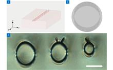
Circular cladding waveguides in Pr:YAG fabricated by femtosecond laser inscription: Raman, luminescence properties and guiding performance
Quanxin Yang, Hongliang Liu, Shan He, Qingyu Tian, Bin Xu, and Pengfei Wu
We report on the fabrication of circular cladding waveguides with cross-section diameters of 60-120 μm in Pr:YAG crystal by applying femtosecond laser inscription. The fabricated waveguides present 2D guidance on the cross-section and fairly low propagation losses. Multiple high-order guiding modes are observed in waveWe report on the fabrication of circular cladding waveguides with cross-section diameters of 60-120 μm in Pr:YAG crystal by applying femtosecond laser inscription. The fabricated waveguides present 2D guidance on the cross-section and fairly low propagation losses. Multiple high-order guiding modes are observed in waveguides with different diameters. Corresponding simulation results reveal the origin of a specific kind of guiding modes. Confocal micro-Raman (μ-Raman) experiments demonstrate the modification effects in femtosecond laser affected areas and ascertain the refractive index induced guiding mechanism. In addition, luminescence emission properties of Pr3+ ions at waveguide volume are well preserved during the femtosecond laser inscription process, which may result in a potential high-power visible waveguide laser..
Opto-Electronic Advances
- Publication Date: Feb. 28, 2021
- Vol. 4, Issue 2, 200005-1 (2021)


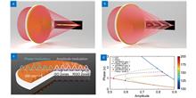
Generation of super-resolved optical needle and multifocal array using graphene oxide metalenses
Hongtao Wang, Chenglong Hao, Han Lin, Yongtian Wang, Tian Lan, Cheng-Wei Qiu, and Baohua Jia
Ultrathin flat metalenses have emerged as promising alternatives to conventional diffractive lenses, offering new possibilities for myriads of miniaturization and interfacial applications. Graphene-based materials can achieve both phase and amplitude modulations simultaneously at a single position due to the modificatiUltrathin flat metalenses have emerged as promising alternatives to conventional diffractive lenses, offering new possibilities for myriads of miniaturization and interfacial applications. Graphene-based materials can achieve both phase and amplitude modulations simultaneously at a single position due to the modification of the complex refractive index and thickness by laser conversion from graphene oxide into graphene like materials. In this work, we develop graphene oxide metalenses to precisely control phase and amplitude modulations and to achieve a holistic and systematic lens design based on a graphene-based material system. We experimentally validate our strategies via demonstrations of two graphene oxide metalenses: one with an ultra-long (~16λ) optical needle, and the other with axial multifocal spots, at the wavelength of 632.8 nm with a 200 nm thin film. Our proposed graphene oxide metalenses unfold unprecedented opportunities for accurately designing graphene-based ultrathin integratable devices for broad applications..
Opto-Electronic Advances
- Publication Date: Feb. 28, 2021
- Vol. 4, Issue 2, 200031-1 (2021)
Review
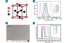
Review of blue perovskite light emitting diodes with optimization strategies for perovskite film and device structure
Zongtao Li, Kai Cao, Jiasheng Li, Yong Tang, Xinrui Ding, and Binhai Yu
Perovskite light emitting diodes (PeLEDs) have attracted considerable research attention because of their external quantum efficiency (EQE) of >20% and have potential scope for further improvement. However, compared to red and green PeLEDs, blue PeLEDs have not been extensively investigated, which limits their commePerovskite light emitting diodes (PeLEDs) have attracted considerable research attention because of their external quantum efficiency (EQE) of >20% and have potential scope for further improvement. However, compared to red and green PeLEDs, blue PeLEDs have not been extensively investigated, which limits their commercial applications in the fields of luminance and full-color displays. In this review, blue-PeLED-related research is categorized by the composition of perovskite. The main challenges and corresponding optimization strategies for perovskite films are summarized. Next, the novel strategies for the design of device structures of blue PeLEDs are reviewed from the perspective of transport layers and interfacial layers. Accordingly, future directions for blue PeLEDs are discussed. This review can be a guideline for optimizing perovskite film and device structure of blue PeLEDs, thereby enhancing their development and application scope..
Opto-Electronic Advances
- Publication Date: Feb. 28, 2021
- Vol. 4, Issue 2, 200019-1 (2021)
© Copyright 2018-2021 | Chinese Laser Press. All Rights Reserved 沪ICP备15018463号-20