• Chinese Optics Letters
  • Vol. 19, Issue 7, 071301 (2021)
Hui Ma1, Haotian Yang1, Bo Tang2, Maoliang Wei1, Junying Li1, Jianghong Wu3、4, Peng Zhang2, Chunlei Sun3、4, Lan Li3、4, and Hongtao Lin1、*
Author Affiliations
  • 1State Key Laboratory of Modern Optical Instrumentation, College of Information Science and Electronic Engineering, Zhejiang University, Hangzhou 310007, China
  • 2Institute of Microelectronics, Chinese Academic Society, Beijing 100029, China
  • 3Key Laboratory of 3D Micro/Nano Fabrication and Characterization of Zhejiang Province, School of Engineering, Westlake University, Hangzhou 310007, China
  • 4Institute of Advanced Technology, Westlake Institute for Advanced Study, Hangzhou 310023, China
  • show less
    DOI: 10.3788/COL202119.071301 Cite this Article Set citation alerts
    Hui Ma, Haotian Yang, Bo Tang, Maoliang Wei, Junying Li, Jianghong Wu, Peng Zhang, Chunlei Sun, Lan Li, Hongtao Lin. Passive devices at 2 µm wavelength on 200 mm CMOS-compatible silicon photonics platform [Invited][J]. Chinese Optics Letters, 2021, 19(7): 071301 Copy Citation Text show less
    Schematic diagram of the measurement system. PR, polarization rotator; DUT, device-under-test; PD, photodetector; TIA, trans-impedance amplifier; DAQ, data acquisition card; PC, personal computer.
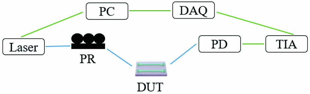
    Fig. 1. Schematic diagram of the measurement system. PR, polarization rotator; DUT, device-under-test; PD, photodetector; TIA, trans-impedance amplifier; DAQ, data acquisition card; PC, personal computer.
    (a) Cross-section diagram of the SOI ridge waveguide. (b) Calculated effective refractive index of the fundamental (black) and first-order (red) TE modes as a function of the ridge waveguide width at 2025 nm. Inset: the spatial distribution of the fundamental and second-order polarized optical modes into the SOI ridge waveguide with a width of 0.6 µm and 1.4 µm at 2025 nm, respectively.
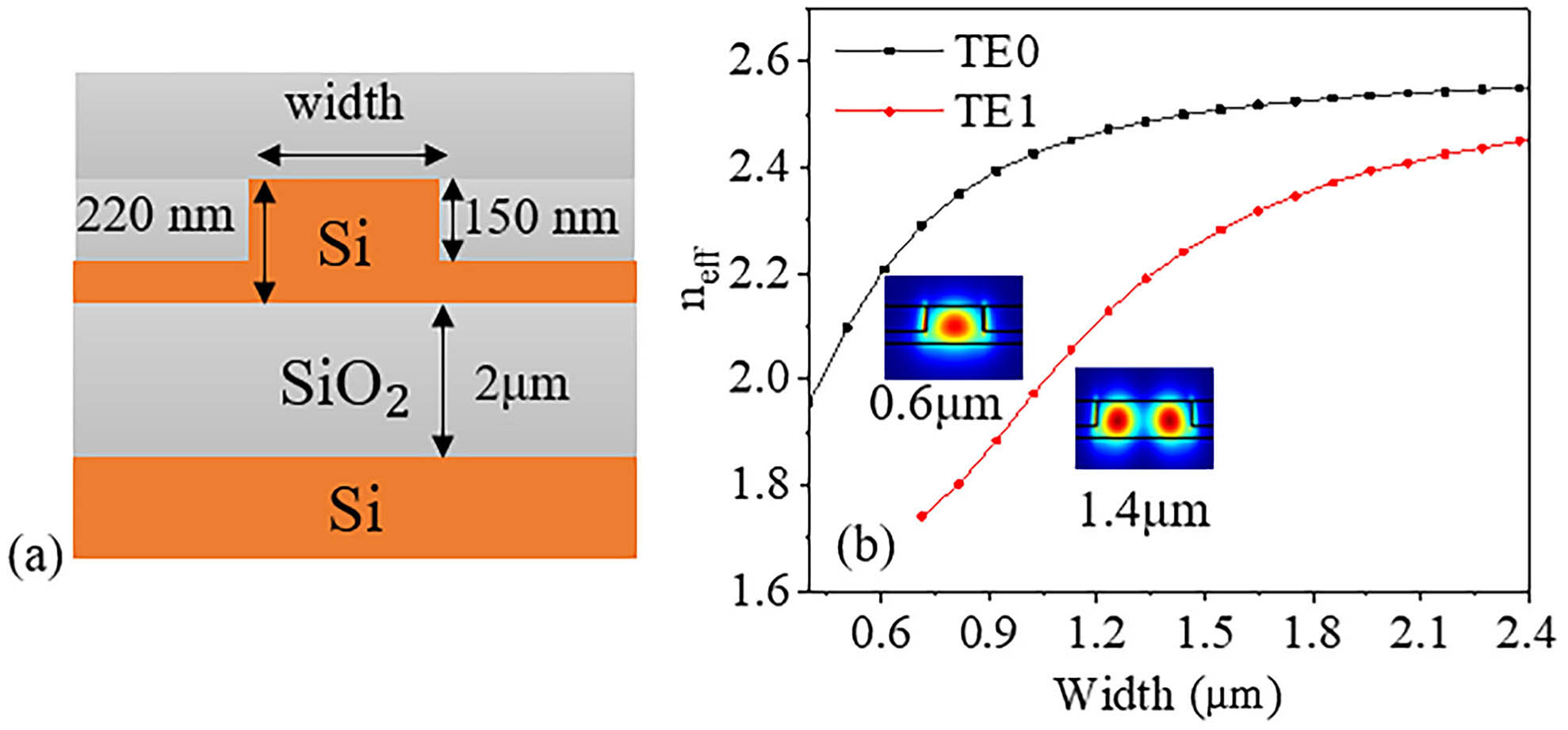
    Fig. 2. (a) Cross-section diagram of the SOI ridge waveguide. (b) Calculated effective refractive index of the fundamental (black) and first-order (red) TE modes as a function of the ridge waveguide width at 2025 nm. Inset: the spatial distribution of the fundamental and second-order polarized optical modes into the SOI ridge waveguide with a width of 0.6 µm and 1.4 µm at 2025 nm, respectively.
    (a) Measured spectral response of an MRR without doping. Inset: enlarged view of the measured resonance peak obtained by Lorentzian fitting and top-view SEM image of the MRR. (b) The measured spectral response of an MRR with light p-type doping.
    Fig. 3. (a) Measured spectral response of an MRR without doping. Inset: enlarged view of the measured resonance peak obtained by Lorentzian fitting and top-view SEM image of the MRR. (b) The measured spectral response of an MRR with light p-type doping.
    (a) Simulated and measured coupling efficiency of the grating coupler. (b) Top-view SEM image of the fabricated GC.
    Fig. 4. (a) Simulated and measured coupling efficiency of the grating coupler. (b) Top-view SEM image of the fabricated GC.
    (a) Simulated transmission spectra of the crossing from port 1 to ports 2 and 3 [the port numbers are shown in (b-2)]. Inset: electric field distribution at 2025 nm. (b) Microscope and SEM images of the cascaded and single crossing. (b-1) Microscope view of cascaded crossing with numbers 15, 30, and 45, and the device structure for crosstalk test; (b-2) enlarged view of the structure for crosstalk test; (b-3) enlarged view of a single crossing. (c) Cut-back measurements for characterizing the insertion loss of crossings. (d) Measurements of the device crosstalk.
    Fig. 5. (a) Simulated transmission spectra of the crossing from port 1 to ports 2 and 3 [the port numbers are shown in (b-2)]. Inset: electric field distribution at 2025 nm. (b) Microscope and SEM images of the cascaded and single crossing. (b-1) Microscope view of cascaded crossing with numbers 15, 30, and 45, and the device structure for crosstalk test; (b-2) enlarged view of the structure for crosstalk test; (b-3) enlarged view of a single crossing. (c) Cut-back measurements for characterizing the insertion loss of crossings. (d) Measurements of the device crosstalk.
    (a) Simulated transmission spectrum of the 1 × 2 MMI at the wavelength of 2005–2035 nm. Inset: electric field distribution at the wavelength of 2020 nm. (b-1) Microscope view of cascaded 1 × 2 MMIs; the white numbers 0–7 represent the port number; (b-2) zoom-in SEM image of 1 × 2 MMI. (c) Measured transmission spectra of the 1 × 2 MMI at the wavelength of 2025 nm. (d) Total insertion losses as a function of the number of cascaded 1 × 2 MMIs at the wavelength range of 2020–2030 nm. The port numbers shown in (c) correspond to the number marked in (b-1), for example, the curve 0-1 shows the transmission spectrum from port 0 to 1.
    Fig. 6. (a) Simulated transmission spectrum of the 1 × 2 MMI at the wavelength of 2005–2035 nm. Inset: electric field distribution at the wavelength of 2020 nm. (b-1) Microscope view of cascaded 1 × 2 MMIs; the white numbers 0–7 represent the port number; (b-2) zoom-in SEM image of 1 × 2 MMI. (c) Measured transmission spectra of the 1 × 2 MMI at the wavelength of 2025 nm. (d) Total insertion losses as a function of the number of cascaded 1 × 2 MMIs at the wavelength range of 2020–2030 nm. The port numbers shown in (c) correspond to the number marked in (b-1), for example, the curve 0-1 shows the transmission spectrum from port 0 to 1.
    (a) Optical image of the fabricated MZI. Ports 1 and 2 represent the input and output ports of the MZI. (b) Measured transmission spectrum of the MZI.
    Fig. 7. (a) Optical image of the fabricated MZI. Ports 1 and 2 represent the input and output ports of the MZI. (b) Measured transmission spectrum of the MZI.
    Hui Ma, Haotian Yang, Bo Tang, Maoliang Wei, Junying Li, Jianghong Wu, Peng Zhang, Chunlei Sun, Lan Li, Hongtao Lin. Passive devices at 2 µm wavelength on 200 mm CMOS-compatible silicon photonics platform [Invited][J]. Chinese Optics Letters, 2021, 19(7): 071301
    Download Citation