
Hui Ma, Haotian Yang, Bo Tang, Maoliang Wei, Junying Li, Jianghong Wu, Peng Zhang, Chunlei Sun, Lan Li, Hongtao Lin, "Passive devices at 2 µm wavelength on 200 mm CMOS-compatible silicon photonics platform [Invited]," Chin. Opt. Lett. 19, 071301 (2021)
- Chinese Optics Letters
- Vol. 19, Issue 7, 071301 (2021)
Abstract
Keywords
1. Introduction
With the development of information technology, the channel capacity of current communication systems based on telecom-wavelength bands is gradually approaching their theoretical limits. The development of new technology will be the key to meeting the increasing demand for high-speed data transmission. Due to the recent advancement of the low-loss hollow-core photonic bandgap fiber[
Complementary metal-oxide-semiconductor (CMOS)-compatible silicon photonic technology offers unique advantages for integrated devices at 2 µm in terms of high performance, large-scale fabrication, and low cost. Recently, some critical devices for this band, including lasers[
In this paper, passive photonic devices operating at 2 µm were fabricated by using the silicon photonic multi-project wafer (MPW) process. A propagation loss of 1.62 dB/cm for ridge waveguides was calculated from MRRs with an intrinsic quality factor around
Sign up for Chinese Optics Letters TOC. Get the latest issue of Chinese Optics Letters delivered right to you!Sign up now
2. Fabrication and Measurement System
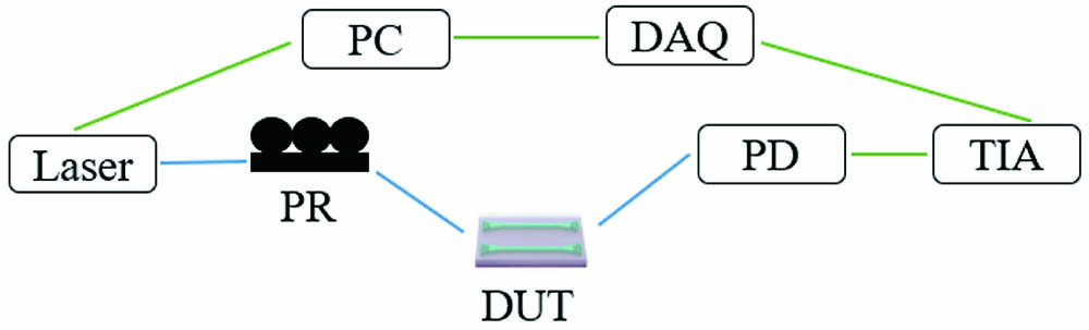
The passive devices were fabricated with the 180 nm silicon photonic MPW process in the Institute of Microelectronics of Chinese Academy of Sciences (IMECAS). The ridge waveguide was etched by 150 nm and cladded by
![]()
Figure 1.Schematic diagram of the measurement system. PR, polarization rotator; DUT, device-under-test; PD, photodetector; TIA, trans-impedance amplifier; DAQ, data acquisition card; PC, personal computer.
3. SOI Passive Devices
3.1. Waveguide and micro-ring resonator
The cross section of the waveguide is shown in Fig. 2(a). To determine the single-mode condition and avoid high-order modes, we simulated the effective refractive index
![]()
Figure 2.(a) Cross-section diagram of the SOI ridge waveguide. (b) Calculated effective refractive index of the fundamental (black) and first-order (red) TE modes as a function of the ridge waveguide width at 2025 nm. Inset: the spatial distribution of the fundamental and second-order polarized optical modes into the SOI ridge waveguide with a width of 0.6 µm and 1.4 µm at 2025 nm, respectively.
MRRs were implemented to characterize the propagation loss of the waveguide. The inset in Fig. 3(a) is the SEM image of the MRR with a diameter of 80 µm. Transmission spectra of MRRs without and with light
![]()
Figure 3.(a) Measured spectral response of an MRR without doping. Inset: enlarged view of the measured resonance peak obtained by Lorentzian fitting and top-view SEM image of the MRR. (b) The measured spectral response of an MRR with light p-type doping.
3.2. Grating coupler
Due to the compact footprint and the convenience of alignment, GCs attracted extensive attention in fiber-to-waveguide couplings. Here, we designed and fabricated a 150 nm etched GC (period 0.985 µm, duty cycle 0.5) with a coupling angle of 8 deg. Based on the Bragg equation, the period of the GC is estimated as below:
![]()
Figure 4.(a) Simulated and measured coupling efficiency of the grating coupler. (b) Top-view SEM image of the fabricated GC.
3.3. Waveguide crossing
Waveguide crossings are basic components for large-scale on-chip optical interconnection. According to the self-imaging theory, many high-performance crossings have been demonstrated in communication wavebands[
![]()
Figure 5.(a) Simulated transmission spectra of the crossing from port 1 to ports 2 and 3 [the port numbers are shown in (b-2)]. Inset: electric field distribution at 2025 nm. (b) Microscope and SEM images of the cascaded and single crossing. (b-1) Microscope view of cascaded crossing with numbers 15, 30, and 45, and the device structure for crosstalk test; (b-2) enlarged view of the structure for crosstalk test; (b-3) enlarged view of a single crossing. (c) Cut-back measurements for characterizing the insertion loss of crossings. (d) Measurements of the device crosstalk.
3.4. Multimode interferometer
In the on-chip photonic system, MMI is one of the fundamental components for optical signal splitting and combining. Here,
![]()
Figure 6.(a) Simulated transmission spectrum of the 1 × 2 MMI at the wavelength of 2005–2035 nm. Inset: electric field distribution at the wavelength of 2020 nm. (b-1) Microscope view of cascaded 1 × 2 MMIs; the white numbers 0–7 represent the port number; (b-2) zoom-in SEM image of 1 × 2 MMI. (c) Measured transmission spectra of the 1 × 2 MMI at the wavelength of 2025 nm. (d) Total insertion losses as a function of the number of cascaded 1 × 2 MMIs at the wavelength range of 2020–2030 nm. The port numbers shown in (c) correspond to the number marked in (b-1), for example, the curve 0-1 shows the transmission spectrum from port 0 to 1.
3.5. Mach–Zehnder interferometer
MZI is a prominent constituent of modulators[
![]()
Figure 7.(a) Optical image of the fabricated MZI. Ports 1 and 2 represent the input and output ports of the MZI. (b) Measured transmission spectrum of the MZI.
4. Conclusion
In summary, we have designed, fabricated, and characterized the fundamental passive silicon photonic components operating in the 2 µm waveband. All devices were etched by 150 nm on a 220 nm thick silicon layer in a silicon photonic MPW process. The propagation loss of the waveguide was 1.62 dB/cm, which was inferred from a ring resonator with an intrinsic quality factor as high as
References
[1] H. Sakr, T. D. Bradley, Y. Hong, G. T. Jasion, J. R. Hayes, H. Kim, I. A. Davidson, E. N. Fokoua, Y. Chen, K. R. H. Bottrill, N. Taengnoi, P. Petropoulos, D. J. Richardson, F. Poletti. Ultrawide bandwidth hollow core fiber for interband short reach data transmission. Optical Fiber Communication Conference Postdeadline Papers 2019, Th4A.1(2019).
[2] Z. Li, A. M. Heidt, J. M. Daniel, Y. Jung, S. U. Alam, D. J. Richardson. Thulium-doped fiber amplifier for optical communications at 2 µm. Opt. Express, 21, 9289(2013).
[3] M. N. Petrovich, F. Poletti, J. P. Wooler, A. M. Heidt, N. K. Baddela, Z. Li, D. R. Gray, R. Slavik, F. Parmigiani, N. V. Wheeler, J. R. Hayes, E. Numkam, L. Gruner-Nielsen, B. Palsdottir, R. Phelan, B. Kelly, J. O’Carroll, M. Becker, N. MacSuibhne, J. Zhao, F. C. Gunning, A. D. Ellis, P. Petropoulos, S. U. Alam, D. J. Richardson. Demonstration of amplified data transmission at 2 µm in a low-loss wide bandwidth hollow core photonic bandgap fiber. Opt Express, 21, 28559(2013).
[4] A. Schliesser, N. Picqué, T. W. Hänsch. Mid-infrared frequency combs. Nat. Photon., 6, 440(2012).
[5] M. C. Estevez, M. Alvarez, L. M. Lechuga. Integrated optical devices for lab-on-a-chip biosensing applications. Laser Photon. Rev., 6, 463(2012).
[6] N. Li, E. S. Magden, Z. Su, N. Singh, A. Ruocco, M. Xin, M. Byrd, P. T. Callahan, J. D. B. Bradley, C. Baiocco, D. Vermeulen, M. R. Watts. Broadband 2-µm emission on silicon chips: monolithically integrated holmium lasers. Opt. Express, 26, 2220(2018).
[7] R. Wang, S. Sprengel, A. Vasiliev, G. Boehm, J. Van Campenhout, G. Lepage, P. Verheyen, R. Baets, M.-C. Amann, G. Roelkens. Widely tunable 2.3 µm III-V-on-silicon Vernier lasers for broadband spectroscopic sensing. Photon. Res., 6, 858(2018).
[8] W. Cao, D. Hagan, D. J. Thomson, M. Nedeljkovic, C. G. Littlejohns, A. Knights, S.-U. Alam, J. Wang, F. Gardes, W. Zhang, S. Liu, K. Li, M. S. Rouifed, G. Xin, W. Wang, H. Wang, G. T. Reed, G. Z. Mashanovich. High-speed silicon modulators for the 2 µm wavelength band. Optica, 5, 1055(2018).
[9] X. Wang, W. Shen, W. Li, Y. Liu, Y. Yao, J. Du, Q. Song, K. Xu. High-speed silicon photonic Mach–Zehnder modulator at 2 µm. Photon. Res., 9, 535(2021).
[10] J. J. Ackert, D. J. Thomson, L. Shen, A. C. Peacock, P. E. Jessop, G. T. Reed, G. Z. Mashanovich, A. P. Knights. High-speed detection at two micrometres with monolithic silicon photodiodes. Nat. Photon., 9, 393(2015).
[11] E. Ryckeboer, A. Gassenq, M. Muneeb, N. Hattasan, S. Pathak, L. Cerutti, J. B. Rodriguez, E. Tournie, W. Bogaerts, R. Baets, G. Roelkens. Silicon-on-insulator spectrometers with integrated GaInAsSb photodiodes for wide-band spectroscopy from 1510 to 2300 nm. Opt. Express, 21, 6101(2013).
[12] S. Zlatanovic, J. S. Park, S. Moro, J. M. C. Boggio, I. B. Divliansky, N. Alic, S. Mookherjea, S. Radic. Mid-infrared wavelength conversion in silicon waveguides using ultracompact telecom-band-derived pump source. Nat. Photon., 4, 561(2010).
[13] X. Liu, B. Kuyken, G. Roelkens, R. Baets, R. M. Osgood, W. M. J. Green. Bridging the mid-infrared-to-telecom gap with silicon nanophotonic spectral translation. Nat. Photon., 6, 667(2012).
[14] H. Subbaraman, X. Xu, A. Hosseini, X. Zhang, Y. Zhang, D. Kwong, R. T. Chen. Recent advances in silicon-based passive and active optical interconnects. Opt. Express, 23, 2487(2015).
[15] N. Hattasan, B. Kuyken, F. Leo, E. M. P. Ryckeboer, D. Vermeulen, G. Roelkens. High-efficiency SOI fiber-to-chip grating couplers and low-loss waveguides for the short-wave infrared. IEEE Photon. Technol. Lett., 24, 1536(2012).
[16] J. Kang, Z. Cheng, W. Zhou, T. H. Xiao, K. L. Gopalakrisna, M. Takenaka, H. K. Tsang, K. Goda. Focusing subwavelength grating coupler for mid-infrared suspended membrane germanium waveguides. Opt. Lett., 42, 2094(2017).
[17] J. Li, Y. Liu, Y. Meng, K. Xu, J. Du, F. Wang, Z. He, Q. Song. 2-µm wavelength grating coupler, bent waveguide, and tunable microring on silicon photonic MPW. IEEE Photon. Technol. Lett., 30, 471(2018).
[18] H. Xie, Y. Liu, W. Sun, Y. Wang, K. Xu, J. Du, Z. He, Q. Song. Inversely designed 1 × 4 power splitter with arbitrary ratios at 2-µm spectral band. IEEE Photon. J., 10, 2700506(2018).
[19] E. J. Stanton, N. Volet, J. E. Bowers. Silicon arrayed waveguide gratings at 2.0-µm wavelength characterized with an on-chip resonator. Opt. Lett., 43, 1135(2018).
[20] M. S. Rouifed, C. G. Littlejohns, G. X. Tina, H. Qiu, J. S. Penades, M. Nedeljkovic, Z. Zhang, C. Liu, D. J. Thomson, G. Z. Mashanovich, G. T. Reed, H. Wang. Ultra-compact MMI-based beam splitter demultiplexer for the NIR/MIR wavelengths of 1.55 µm and 2 µm. Opt. Express, 25, 10893(2017).
[21] S. Zheng, M. Huang, X. Cao, L. Wang, Z. Ruan, L. Shen, J. Wang. Silicon-based four-mode division multiplexing for chip-scale optical data transmission in the 2 µm waveband. Photon. Res., 7, 1030(2019).
[22] L. Zhang, L. Jie, M. Zhang, Y. Wang, Y. Xie, Y. Shi, D. Dai. Ultrahigh-Q silicon racetrack resonators. Photon. Res., 8, 684(2020).
[23] H. Liu, H. Tam, P. K. A. Wai, E. Pun. Low-loss waveguide crossing using a multimode interference structure. Opt. Commun., 241, 99(2004).
[24] Y. Ma, Y. Zhang, S. Yang, A. Novack, R. Ding, A. E. Lim, G. Q. Lo, T. Baehr-Jones, M. Hochberg. Ultralow loss single layer submicron silicon waveguide crossing for SOI optical interconnect. Opt. Express, 21, 29374(2013).
[25] M. Johnson, M. G. Thompson, D. Sahin. Low-loss, low-crosstalk waveguide crossing for scalable integrated silicon photonics applications. Opt. Express, 28, 12498(2020).
[26] D. J. Thomson, F. Y. Gardes, J.-M. Fedeli, S. Zlatanovic, Y. Hu, B. P. P. Kuo, E. Myslivets, N. Alic, S. Radic, G. Z. Mashanovich, G. T. Reed. 50-Gb/s silicon optical modulator. IEEE Photon. Technol. Lett., 24, 234(2012).
[27] X. Tu, T. Y. Liow, J. Song, X. Luo, Q. Fang, M. Yu, G. Q. Lo. 50-Gb/s silicon optical modulator with traveling-wave electrodes. Opt. Express, 21, 12776(2013).
[28] N. Youngblood, Y. Anugrah, R. Ma, S. J. Koester, M. Li. Multifunctional graphene optical modulator and photodetector integrated on silicon waveguides. Nano Lett., 14, 2741(2014).
[29] Y. Shoji, K. Kintaka, S. Suda, H. Kawashima, T. Hasama, H. Ishikawa. Low-crosstalk 2 × 2 thermo-optic switch with silicon wire waveguides. Opt. Express, 18, 9071(2010).
[30] Y. Ding, M. Pu, L. Liu, J. Xu, C. Peucheret, X. Zhang, D. Huang, H. Ou. Bandwidth and wavelength-tunable optical bandpass filter based on silicon microring-MZI structure. Opt. Express, 19, 6462(2011).


Set citation alerts for the article
Please enter your email address

© Copyright 2018-2021 | Chinese Laser Press. All Rights Reserved 沪ICP备15018463号-20