• Journal of Semiconductors
  • Vol. 40, Issue 1, 012805 (2019)
Jianjun Shi, Xiaochuan Xia, Qasim Abbas, Jun Liu, Heqiu Zhang, Yang Liu, and Hongwei Liang
Author Affiliations
  • School of Microelectronics, Dalian University of Technology, Dalian 116024, China
  • show less
    DOI: 10.1088/1674-4926/40/1/012805 Cite this Article
    Jianjun Shi, Xiaochuan Xia, Qasim Abbas, Jun Liu, Heqiu Zhang, Yang Liu, Hongwei Liang. Current transport mechanism of Mg/Au ohmic contacts to lightly doped n-type β-Ga2O3[J]. Journal of Semiconductors, 2019, 40(1): 012805 Copy Citation Text show less

    Abstract

    The carrier transport mechanism of Mg/Au ohmic contact for lightly doped β-Ga2O3 is investigated. An excellent ohmic contact has been achieved when the sample was annealed at 400 °C and the specific contact resistance is 4.3 × 10⁻⁴ Ω·cm2. For the annealed sample, the temperature dependence of specific contact resistance is studied in the range from 300 to 375 K. The specific contact resistance is decreased from 4.3 × 10⁻⁴ to 1.59 × 10⁻⁴ Ω·cm2 with an increase of test temperature. As combination with the judge of E00, the basic mechanism of current transport is dominant by thermionic emission theory. The effective barrier height between Mg/Au and β-Ga2O3 is evaluated to be 0.1 eV for annealed sample by fitting experimental data with thermionic emission model.

    1. Introduction

    Beta gallium oxide (β-Ga2O3), with a large band gap of about 4.8 eV and a high theoretical breakdown electric field of 8 MV/cm[1, 2], has gained prominent attention to be applied as an adequate material for high power electronic devices. The Baliga’s figure of merit for β-Ga2O3 is about ten times larger than that of 4H-SiC and four times larger than that of GaN[3]. Another important advantage of β-Ga2O3 is that larger-area single-crystal substrates can be synthesized by several conventional melt growth methods, commonly employed are Czochralski (CZ)[4, 5], floating-zone (FZ)[6, 7], and edge-defined film-fed growth (EFG)[810]. In addition, carrier concentration of n-type β-Ga2O3 can be controlled by doping with Sn/Si in range of 1015–1019 cm−3[11, 12].

    The metal oxide semiconductor field-effect transistors (MOSFET) and schottky barrier diodes are two critical power electronics application of β-Ga2O3. Low resistance ohmic contacts are essential for β-Ga2O3 devices to reduce devices’ conduction loss. Several groups[1315] have employed heavily doping by ion implantation technique and an intermediate semiconductor layer between metal and semiconductor to form ohmic contact. However, both of them were either expensive or complex. Additionally, in spite of the resistance of ohmic contacts per unit area being as low as 4.6 × 10⁻⁶ Ω·cm2, the mechanism of current transport in β-Ga2O3 ohmic contacts has received a little attention and is reported rarely. The current transport mechanism is vital for improving performance of β-Ga2O3-based powder devices to understand the basic electrical characteristic of ohmic contact on β-Ga2O3 surface, including Schottky barrier height and the carrier transport mechanism.

    Up till now, four leading model of current flow in the metal–semiconductor ohmic contact are developed, namely, the thermionic emission theory (TE), field emission (FE), thermal-field emission theory (TFE), and metallic shunts model[16]. The E00 is defined as qh/4π[N/(m*εs)]1/2. Here, h is the Plank constant, N is carrier concentration in the semiconductor, εs is the permittivity of the semiconductor, q is the elementary charge, and m* is the effective mass of electron in the semiconductor. (Ⅰ) For thermionic emission theory, , the specific contact resistance (ρc) of the ohmic contact decreases with increasing temperature and rises exponentially with an increase in φb between metal and semiconductor. Here, k is Boltzmann constant and φb is the effect barrier height between metal and semiconductor. (Ⅱ) For field emission theory, , ρC increases with φb and decrease with increasing carrier concentration of uncompensated impurities in a semiconductor, and is virtually independent of the temperature. (Ⅲ) For thermal-field emission theory, , ρc should increase with an increase in φb and weakly decreases with an increase of temperature. (Ⅳ) For metallic shunts model, ρC increases with temperature. In addition, there is another criterion for judging in which current transport model is dominant: when qE00/kT < 0.5, the thermal emission mechanism is dominant; when qE00/kT > 5, the field emission is dominant; when 0.5 < qE00/kT < 5, the thermionic field emission is dominant.

    In this letter, Mg/Au is used to prepare ohmic contact with lightly doped β-Ga2O3 because of its low work function, high humidity resistance, oxygen resistance, and corrosion resistance[17, 18]. The Mg/Au stacks exhibit excellent ohmic contact properties on lightly doped β-Ga2O3 after annealing at 400 °C. To investigate current transport mechanism on β-Ga2O3, the dependence of current–voltage on measuring temperature was performed, followed by an analysis based on TE model.

    2. Experimental

    The Sn lightly doped ( 01)-oriented β-Ga2O3 substrate with 680 μm thickness was used by cutting into 5 × 5 mm2 pieces. The carrier concentration of single crystal β-Ga2O3 substrate was about 4.94 × 1017 cm−3. Prior to metal deposition, the substrate was cleaned in methanol, acetone, methanol, and deionized water (DIW) by ultra-sonication for 5 minutes, respectively. Next, the substrates were dipped in Piranha solutions (DIW (30 %) : H2O2 (96%) : H2SO4 = 1 : 1 : 4) solution for 5 min. Then, the substrates were dipped in DIW at 90 °C for 5 min, later cooled down to room temperature. Finally, the substrate was rinsed in HF (> 40%) for 5 h. Metal deposition was performed by conventional thermal evaporation method. The Mg metal (99.999%) was evaporated with the thickness of 820 nm, followed by 600 nm thick Au metal film coating. Then metal electrodes were annealed at an optimum temperature of 400 °C for 2 min in a quartz tube under Ar gas protection. The contact metal pads for transmission line method (TLM) testers were formed by standard lithography process with space of 0.15, 0.2, 0.25, 0.3, and 0.4 mm. The dimensions of contact metal pads are 0.4 × 1.2 mm2.

    The current–voltage characteristics were measured using Keithley 2611A semiconductor characterization system in the range of 300–375 K. The ρc was extracted using the transmission line method (TLM). Hall Effect 5500 PC measurement system was employed to determine the carrier concentration of bulk β-Ga2O3.

    3. Results and discussion

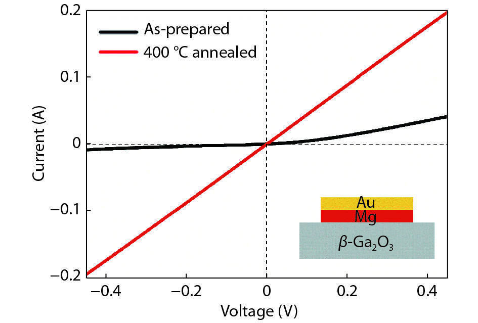
    Fig. 1 shows the current–voltage characteristics of as-deposited and annealed Mg/Au/β-Ga2O3 contacts samples, as measured from adjacent contact pads with a gap spacing of 0.15 mm. For the as-prepared sample, the I–V curves showed nonlinear behavior, while sample annealed at 400 °C showed the linear behavior of current–voltage curve, which indicates that thermal annealing can lead to the formation of ohmic contacts.

    (Color online) I–V curves for as-prepared and 400 °C annealed samples. The insert is the schematic structure of the Mg/Au/β-Ga2O3 contact.

    Figure 1.(Color online) I–V curves for as-prepared and 400 °C annealed samples. The insert is the schematic structure of the Mg/Au/β-Ga2O3 contact.

    Suzuki et al.[19] reported that the barrier height of Au/β-Ga2O3 contact decreased with an increase in the annealing temperature. Similarly, in our experiment, the annealing results in lowing the barrier height between Mg/Au and β-Ga2O3 interfaces and formed ohmic contact to show linear I–V characteristic.

    Fig. 2(a) shows the dependence of the experimentally measured total resistance (RT) on distance (d) between two adjacent contact pads for the annealed sample at different measuring temperatures. The RT can be represented by equation:

    ${R_ {\rm{T}}} = 2{R_ {\rm{C}}} + \displaystyle\frac{{d{R_{\rm SH}}}}{W} = 2{R_ {\rm{C}}} + \frac{d}{{qN{\mu _ {\rm{n}}}S}}. $ ()

    Here, RC and RSH are contact resistance and sheet resistance, respectively. The d, W, q, N, μn and S are the distance of adjacent electrodes, width of electrodes, element charge, carrier concentration, carrier mobility and electrode area, respectively. The intercept of line with the ordinate axis corresponds to double RC and its slope is proportional to the RSH. The dependence of RT on d is linear at each measuring temperature, as shown in Fig. 2(a). Fig. 2(b) shows that the RC decreases from 0.96 to 0.8 Ω and RSH increases from 0.3 to 0.56 Ω/□ as measuring temperature rise from 300 to 375 K. As we know, the carrier mobility is affected by temperature and it decrease with increasing measuring temperature at high temperature. Thus, the reason of the increase of RSH with increasing the testing temperature could be attributed to the decrease of electron mobility.

    (Color online) (a) Resistance of Mg/Au-β-Ga2O3 structure with two adjacent ohmic contacts versus the distance at different temperatures. (b) Contact resistance and sheet resistance of the ohmic contact Mg/Au-β-Ga2O3 versus measuring temperatures.

    Figure 2.(Color online) (a) Resistance of Mg/Au-β-Ga2O3 structure with two adjacent ohmic contacts versus the distance at different temperatures. (b) Contact resistance and sheet resistance of the ohmic contact Mg/Au-β-Ga2O3 versus measuring temperatures.

    In order to investigate the current transport mechanism of Mg/Au ohmic contact for annealed sample, the ρc was extracted as a function of measuring temperature. The ρc decreased slightly from 4.3 × 10⁻⁴ to 1.59 × 10⁻⁴ Ω·cm2 in the measuring temperature range from 300 to 375 K, as shown in Fig. 3. According the model of current flow in the metal semiconductor ohmic contact, TFE and FE model may be the basic theories of current transport at the Mg/Au-β-Ga2O3 ohmic contact interface. However, judging from E00, it is calculated to be 0.007 V and qE00/kT (T = 300 K) is 0.27 < 0.5. Where, the m* is 0.28me[20], εS is 10 for β-Ga2O3, with N is 4.94 × 1017 cm−3 measured by Hall Effect 5500 PC measurement system. Consideration with the lightly doped β-Ga2O3, it is reasonable to conclude that the mechanism of current transport is dominated by thermionic emission theory in the present system rather than thermal-field emission theory.

    (Color online) Specific contact resistance of the ohmic contact Mg/Au-β-Ga2O3 versus measuring temperatures.

    Figure 3.(Color online) Specific contact resistance of the ohmic contact Mg/Au-β-Ga2O3 versus measuring temperatures.

    For FE theory, , the dependence of ρcT on 1/T should be linear on a semi-logarithmic scale with the slope of this dependence proportional to the barrier height φb. Fig. 4 gives the experimental and theoretical relationships between ρcT and 1/T. It is fitted well between them, which means that the current transport mechanism of Mg/Au/β-Ga2O3 ohmic contact is FE consistent with the previous discussion. In addition, the effective barrier height is calculated to be 0.1 eV from the slope of the fitting curve. The effective barrier height between Mg/Au and β-Ga2O3 is sufficiently low which is responsible for the formation of the low contact resistance.

    (Color online) The dependence of ln (ρcT) on 1/T graph about Mg/Au-β-Ga2O3 ohmic contact for the annealed sample, experimental data (point) and TE model fitting (line).

    Figure 4.(Color online) The dependence of ln (ρcT) on 1/T graph about Mg/Au-β-Ga2O3 ohmic contact for the annealed sample, experimental data (point) and TE model fitting (line).

    4. Conclusion

    In summary, ohmic contact has been successfully realized on β-Ga2O3 using low work function Mg/Au stacks after annealing at 400 °C and the current transport mechanism was investigated. The temperature dependence of specific contact resistance of the Mg/Au-β-Ga2O3 ohmic contact decreased with increasing the measuring temperature from 300 to 375 K and qE00/kT is 0.27 < 0.5. Therefore, the current transport mechanism is dominant thermionic emission theory. The effective barrier height extracted is 0.1 eV by fitting experiment data with thermionic emission model. Further investigation will be carried out on the heavily doped β-Ga2O3.

    Acknowledgements

    This work was supported by the National Key R&D Plan (Nos. 2016YFB0400600, 2016YFB0400601),the National Science Foundation of China (Nos. 11675198, 61376046, 11405017, 61574026), the Fundamental Research Funds for the Central Universities (Nos. DUT15LK15, DUT15RC(3)016, No. DUT16LK29), the Liaoning Provincial Natural Science Foundation of China (Nos. 2014020004, 201602453, 201602176), the China Postdoctoral Science Foundation Funded Project (No. 2016M591434), the Open Fund of the State Key Laboratory on Integrated Optoelectronics (Nos. IOSKL2015KF18, IOSKL2015KF22).

    References

    [1]

    [2] M Higashiwaki, K Sasaki, A Kuramata et al. Gallium oxide (Ga2O3) metal–semiconductor field-effect transistors on single-crystal β-Ga2O3 (010) substrates. Appl Phys Lett, 100, 013504(2012).

    [3] M Higashiwaki, K Sasaki, H Murakami et al. Recent progress in Ga2O3 power devices. Semicond Sci Technol, 31, 034001(2016).

    [4] K Irmscher, Z Galazka, M Pietsch et al. Electrical properties of β-Ga2O3 single crystals grown by the Czochralski method. J Appl Phys, 110, 063720(2011).

    [5] Z Galazka, R Uecker, K Irmscher et al. Czochralski growth and characterization of beta-Ga2O3 single crystals. Cryst Res Technol, 45, 1229(2010).

    [6] E G Víllora, K Shimamura, Y Yoshikawa et al. Large-size β-Ga2O3 single crystals and wafers. J Cryst Growth, 270, 420(2004).

    [7] N Ueda, H Hosono, R Waseda et al. Synthesis and control of conductivity of ultraviolet transmitting β-Ga2O3 single crystals. Appl Phys Lett, 70, 3561(1997).

    [8] A Kuramata, K Koshi, S Watanabe et al. High-quality beta-Ga2O3 single crystals grown by edge-defined film-fed growth. Jpn J Appl Phys, 55, 1202A(2016).

    [9] H. Aida, K. Nishiguchi, H. Takeda et al. Growth of beta-Ga2O3 single crystals by the edge-defined, film fed growth method. Jpn J Appl Phys, 47, 8506(2008).

    [10] W Mu, Z Jia, Y Yin et al. High quality crystal growth and anisotropic physical characterization of beta-Ga2O3 single crystals grown by EFG method. J Alloys Compnds, 714, 453(2017).

    [11] K Sasaki, A Kuramata, T Masui et al. Device-quality beta-Ga2O3 epitaxial films fabricated by ozone molecular beam epitaxy. Appl Phys Express, 5, 035502(2012).

    [12] E G Víllora, K Shimamura, Y Yoshikawa et al. Electrical conductivity and carrier concentration control in β-Ga2O3 by Si doping. Appl Phys Lett, 92, 202120(2008).

    [13] K Sasaki, M Higashiwaki, A Kuramata et al. Si-ion implantation doping in beta-Ga2O3 and its application to fabrication of low-resistance ohmic contacts. Appl Phys Express, 6, 086502(2013).

    [14] P H Carey, J Yang, F Ren et al. Ohmic contacts on n-type beta- Ga2O3 using AZO/Ti/Au. AIP Adv, 7, 095313(2017).

    [15] P H Carey, Y Jiancheng, R Fan et al. Improvement of ohmic contacts on Ga2O3 through use of ITO-interlayers. J Vac Sci Technol B, 35, 061201(2017).

    [16] T V Blank, Y A Goldberg, E A Posse. Flow of the current along metallic shunts in ohmic contacts to wide-gap III–V semiconductors. Semiconductors, 43, 1164(2009).

    [17] T Oyamada, H Sasabe, C Adachi. Formation of MgAu alloy cathode by photolithography and its application to organic light-emitting diodes and organic field effect transistors. Electr Eng Jpn, 152, 37-42(2005).

    [18] H Arai, H Nakanotani, K Morimoto et al. Magnesium-gold binary alloy for organic light-emitting diodes with high corrosion resistance. J Vac Sci Technol B, 34, 040607(2016).

    [19] R Suzuki, S Nakagomi, Y Kokubun et al. Enhancement of responsivity in solar-blind β-Ga2O3 photodiodes with a Au Schottky contact fabricated on single crystal substrates by annealing. Appl Phys Lett, 94, 222102(2009).

    [20] S Knight, A Mock, R Korlacki et al. Electron effective mass in Sn-doped monoclinic single crystal beta-gallium oxide determined by mid-infrared optical Hall effect. Appl Phys Lett, 112, 012103(2018).

    Jianjun Shi, Xiaochuan Xia, Qasim Abbas, Jun Liu, Heqiu Zhang, Yang Liu, Hongwei Liang. Current transport mechanism of Mg/Au ohmic contacts to lightly doped n-type β-Ga2O3[J]. Journal of Semiconductors, 2019, 40(1): 012805
    Download Citation