• Photonics Research
  • Vol. 10, Issue 11, 2448 (2022)
Zhenzhao Guo1、2, Jinbiao Xiao2、3、*, and Shengbao Wu1、4、*
Author Affiliations
  • 1Photonics Information Innovation Center, Hebei Provincial Center for Optical Sensing Innovations, College of Physics Science and Technology, Hebei University, Baoding 071002, China
  • 2National Research Center for Optical Sensing/Communications Integrated Networking, School of Electronic Science and Engineering, Southeast University, Nanjing 210096, China
  • 3e-mail:
  • 4e-mail:
  • show less
    DOI: 10.1364/PRJ.470827 Cite this Article Set citation alerts
    Zhenzhao Guo, Jinbiao Xiao, Shengbao Wu. Ultracompact, polarization-independent, and highly scalable optical power splitting model employing fan-out bending metamaterials[J]. Photonics Research, 2022, 10(11): 2448 Copy Citation Text show less
    A 3D schematic of the proposed power splitting scheme: (a) the 1×4 power splitter with enlarged views of light propagation profiles for TE and TM modes, respectively; (b) the top view of the input taper, angled output tapers, and FBSWGs, which are shown separately to facilitate the understanding; the designed (c) 1×2 power splitter, (d) 1×3 power splitter, and (e) 1×5 power splitter. All devices are covered by up-SiO2 claddings, which are not shown here for clarity. (f) Working principle of power splitters using FBSWGs, the optical path from the center point to the arbitrary point of the mth bending grating line is noRm, resulting in curved wavefronts, and such curved wavefronts are matched with that of angled output tapers. Comparisons of (g) conventional straight SWGs and (h) a bending silicon waveguide with the proposed FBSWG scheme. Distributions of electric-fields Ex and Ey for TE and TM modes are also simulated by the 3D-FDTD method and displayed in (f)–(h).
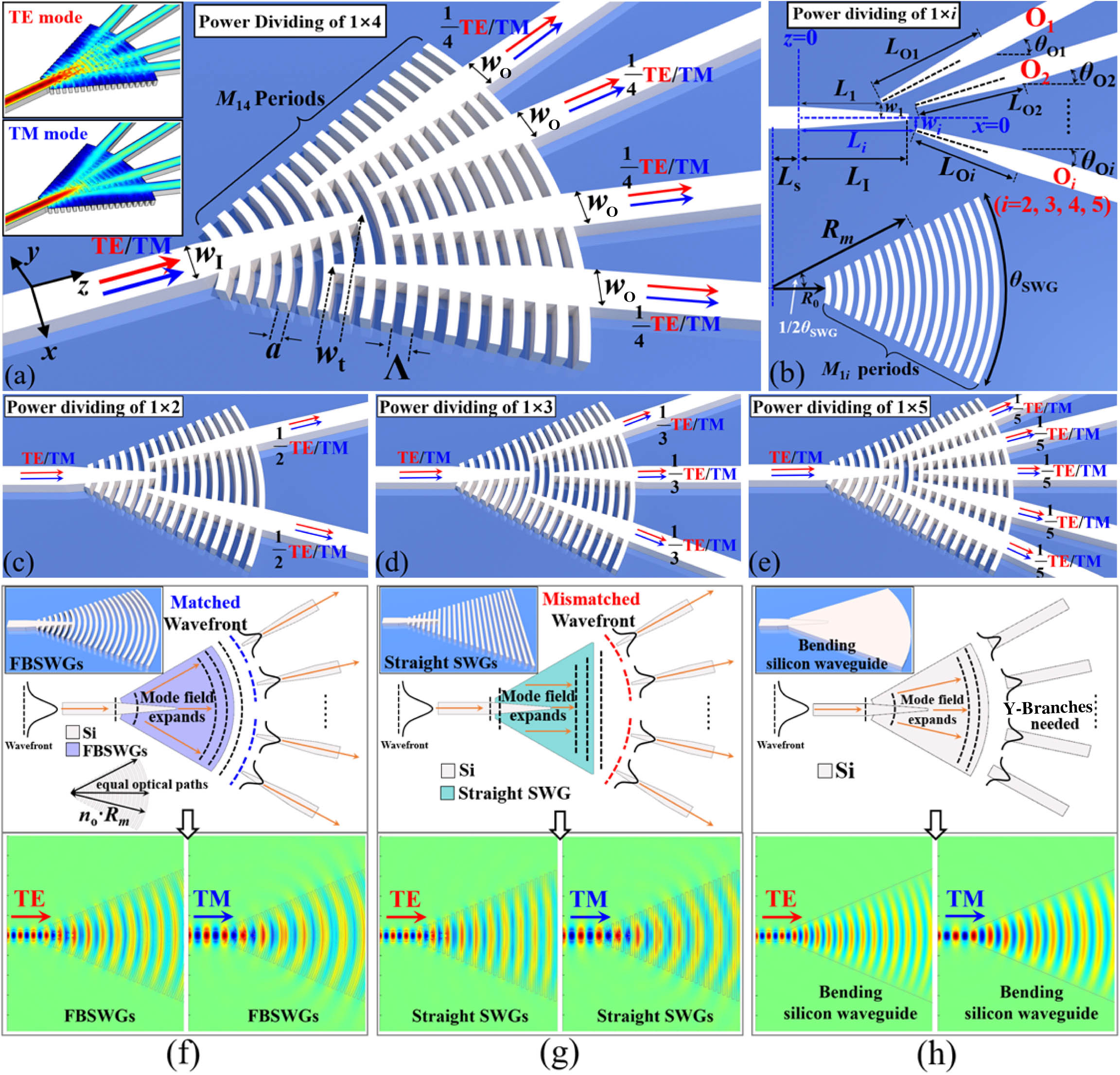
    Fig. 1. A 3D schematic of the proposed power splitting scheme: (a) the 1×4 power splitter with enlarged views of light propagation profiles for TE and TM modes, respectively; (b) the top view of the input taper, angled output tapers, and FBSWGs, which are shown separately to facilitate the understanding; the designed (c) 1×2 power splitter, (d) 1×3 power splitter, and (e) 1×5 power splitter. All devices are covered by up-SiO2 claddings, which are not shown here for clarity. (f) Working principle of power splitters using FBSWGs, the optical path from the center point to the arbitrary point of the mth bending grating line is noRm, resulting in curved wavefronts, and such curved wavefronts are matched with that of angled output tapers. Comparisons of (g) conventional straight SWGs and (h) a bending silicon waveguide with the proposed FBSWG scheme. Distributions of electric-fields Ex and Ey for TE and TM modes are also simulated by the 3D-FDTD method and displayed in (f)–(h).
    Calculated PSDs, respectively, for (a) the TE mode and (b) TM mode as θO1/θO4 and θO2/θO3 vary in Step I, for (c) the TE mode and (d) TM mode as w1/w4 and w2/w3 vary in Step II, for (e) the TE mode and (f) TM mode as L1/L4 and L2/L3 vary in Step III, and for (g) the TE mode and (h) TM mode as LO1/LO4 and LO2/LO3 vary in Step IV.
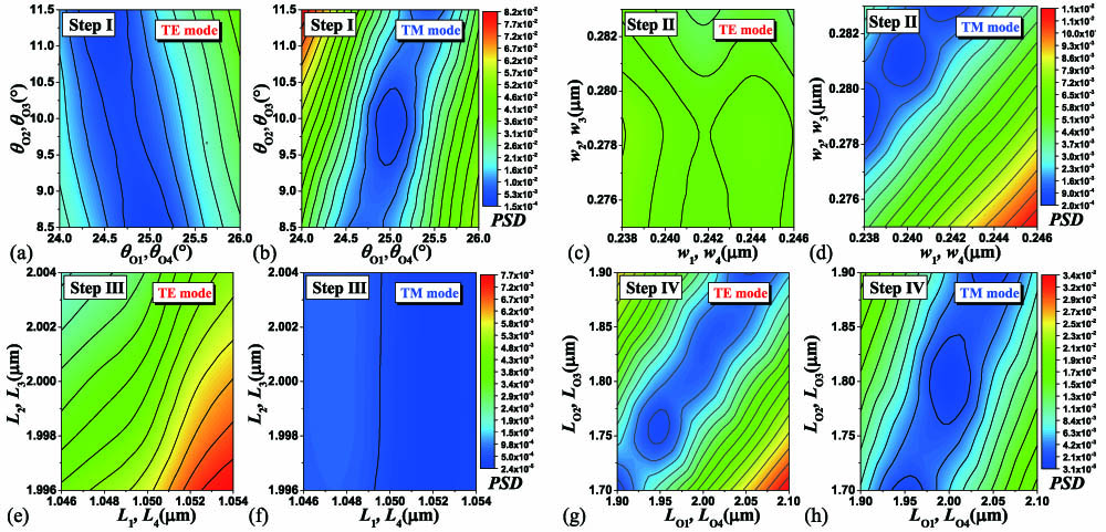
    Fig. 2. Calculated PSDs, respectively, for (a) the TE mode and (b) TM mode as θO1/θO4 and θO2/θO3 vary in Step I, for (c) the TE mode and (d) TM mode as w1/w4 and w2/w3 vary in Step II, for (e) the TE mode and (f) TM mode as L1/L4 and L2/L3 vary in Step III, and for (g) the TE mode and (h) TM mode as LO1/LO4 and LO2/LO3 vary in Step IV.
    Calculated light propagation profiles as the fundamental TE/TM mode is injected for the (a) and (b) 1×2 power splitter, (c) and (d) 1×3 power splitter, (e) and (f) 1×4 power splitter, and (g) and (h) 1×5 power splitter, respectively.
    Fig. 3. Calculated light propagation profiles as the fundamental TE/TM mode is injected for the (a) and (b) 1×2 power splitter, (c) and (d) 1×3 power splitter, (e) and (f) 1×4 power splitter, and (g) and (h) 1×5 power splitter, respectively.
    Calculated ILs and OUs for the (a) 1×3 power splitter, (b) 1×4 power splitter, and (c) 1×5 power splitter with a deviated duty cycle for both TE and TM modes. The calculated wavelength dependence of the ILs and OUs for the (d) 1×3 power splitter, (e) 1×4 power splitter, and (f) 1×5 power splitter for TE and TM polarizations.
    Fig. 4. Calculated ILs and OUs for the (a) 1×3 power splitter, (b) 1×4 power splitter, and (c) 1×5 power splitter with a deviated duty cycle for both TE and TM modes. The calculated wavelength dependence of the ILs and OUs for the (d) 1×3 power splitter, (e) 1×4 power splitter, and (f) 1×5 power splitter for TE and TM polarizations.
    (a) Microscope image of the reference TE and TM waveguides. (b) Microscope image of the three-stage cascaded measure scheme for the fabricated 1×3 power splitters and (c) and (d) corresponding scanning electron microscope (SEM) images of fabricated 1×3 power splitters. Microscope image of the three-stage cascaded measure scheme for the fabricated (e) 1×4 power splitters and (f) 1×5 power splitters. Pseudocolor SEM images of (g) the 1×4 and (h) the 1×5 power splitting elements.
    Fig. 5. (a) Microscope image of the reference TE and TM waveguides. (b) Microscope image of the three-stage cascaded measure scheme for the fabricated 1×3 power splitters and (c) and (d) corresponding scanning electron microscope (SEM) images of fabricated 1×3 power splitters. Microscope image of the three-stage cascaded measure scheme for the fabricated (e) 1×4 power splitters and (f) 1×5 power splitters. Pseudocolor SEM images of (g) the 1×4 and (h) the 1×5 power splitting elements.
    Measured and normalized transmittance Tchannel i spectra of the 1×3 power splitter for the input (a) TE and (b) TM modes, the 1×4 power splitter for the input (c) TE and (d) TM modes, and the 1×5 power splitter for the input (e) TE and (f) TM modes, respectively.
    Fig. 6. Measured and normalized transmittance Tchanneli spectra of the 1×3 power splitter for the input (a) TE and (b) TM modes, the 1×4 power splitter for the input (c) TE and (d) TM modes, and the 1×5 power splitter for the input (e) TE and (f) TM modes, respectively.
    OPSM12θSWGL1L2w1w2θ1θ2LO1LO2R0
    1×217331.31.30.250.25882.42.40.98
    1×3M13θSWGL1L2L3w1w2w3θ1θ2θ3
    19481.692.251.690.400.415.75015.75
    LO1LO2LO3R0
    2.21.952.20.76
    1×4M14θSWGL1L2L3L4w1w2w3w4θ1
    18561.048221.0480.2440.2810.2810.24425
    θ2θ3θ4LO1LO2LO3LO4R0
    9.59.52521.81.820.76
    1×5M15θSWGL1L2L3L4L5w1w2w3w4
    19561.051.9232.251.9231.050.2460.19300.193
    w5θ1θ2θ3θ4θ5LO1LO2LO3LO4LO5
    0.24624.516.5016.525.521.9521.952
    R0
    0.76
    SPCbwIwOwtLsLIaΛ
    0.50.50.10.61.820.120.22
    Table 1. Optimized Parameters of the 1×2, 1×3, 1×4, and 1×5 Power Splittersa
    StructureFunctionLength (µm)IL (dB)OU (dB)Bandwidth (nm)c
    SimaExpbSimExpSimExp
    Y-branch [11]1×4 at TE40000.26<1.2<2.2100 (IL<1)100 (IL<1.2, OU<2.2)
    1×4 at TM<1.8100 (IL<1.3)100 (IL<1.8, OU<2.2)
    Tapers [17]1×4 at TE12.50.18<0.4<0.68100 (IL<0.22)40 (IL<0.4, OU<0.68)
    MMI [20]1×4 at TE360.10.420.080.61150 (IL<0.59, OU<0.34)104 (IL<0.89, OU<0.62)
    DCs [22]1×3 at TE7.30.0160.0680.058<1111 (IL<0.031, OU<1)50 (IL<0.82, OU<1)
    1×3 at TM0.0650.620.021<190 (IL<0.17, OU<1)54 (IL<1.5, OU<1)
    This work1×3 at TE4.240.430.750.0230.64180 (IL<0.6, OU<1)54 (IL<1.2, OU<0.9)
    1×3 at TM0.240.580.0150.32
    1×4 at TE4.020.331.160.0660.8190 (IL<0.6, OU<1)49 (IL<1.35, OU<1)
    1×4 at TM0.180.660.00050.43
    Table 2. Comparison of Several Power Splitters at the Wavelength of 1.55 μm
    Zhenzhao Guo, Jinbiao Xiao, Shengbao Wu. Ultracompact, polarization-independent, and highly scalable optical power splitting model employing fan-out bending metamaterials[J]. Photonics Research, 2022, 10(11): 2448
    Download Citation