1Photonics Information Innovation Center, Hebei Provincial Center for Optical Sensing Innovations, College of Physics Science and Technology, Hebei University, Baoding 071002, China
2National Research Center for Optical Sensing/Communications Integrated Networking, School of Electronic Science and Engineering, Southeast University, Nanjing 210096, China
Optical power splitters (OPSs) are essential components in the photonic integrated circuits. Considerable power splitting schemes have been reported on the silicon-on-insulator platform. However, the corresponding device lengths are enlarged, and polarization-sensitive operations are usually encountered when the splitting channels are increased from two to five. In this paper, a novel power splitting model is proposed to overcome these limitations. Here, fan-out bending subwavelength grating (FBSWG) metamaterials instead of classical straight SWGs are leveraged to expand the input TE/TM mode in an ultracompact region and further bend its wavefronts. By using -angled tapers to match bending wavefronts, the light expanded by FBSWGs can be collected and evenly distributed into output channels. Based on such a model, three OPSs are designed and experimentally demonstrated, which are the shortest polarization-independent , , and OPSs reported until now to our knowledge. The characterizations show low insertion losses (, , and ) and uniformities (, , and ) over bandwidths of 54 nm, 49 nm, and 38 nm for the , , and OPSs, respectively. For the first time, an ultracompact device length of μ and a polarization-independent operation can be maintained simultaneously as the output splitting channels are increased.
1. INTRODUCTION
Silicon photonics based on the silicon-on-insulator (SOI) platform, offering a high index contrast between the silicon core and its surroundings for strong mode field confinement and light-matter interaction, is a promising technology for realizing ultracompact devices in the high-density photonic integrated circuits (PICs) [1]. As fundamental and indispensable building elements serving the purpose of power distribution (1-to- channels), optical power splitters (OPSs) have been broadly utilized in light manipulation and/or forming complex on-chip devices, e.g., optical modulators [2,3], sensors [4], optical phased arrays [5], switches [6], and logic circuits [7]. Over recent years, Y-branches [8], directional couplers (DCs) [9], and multimode interference (MMI) couplers [10] are three main methods towards the realization of on-chip power splitters. Among them, Y-branches, composed of two output branches with an extremely small branching angle, require stringent fabrication processes and rather long device lengths (μ) due to a typical loss figure of 1 dB with a branching angle of [11]. As an alternative, DCs in which two or three silicon nanowires are assembled in parallel are popular options, owing to their structural simplicity. However, the wavelength sensitivity brought by the strict phase-matching condition [12], limits their applications for broadband PICs. MMI couplers based on the self-imaging effect as another approach, seem to be superior candidates in terms of the large fabrication tolerance and broadband operation, but they normally suffer from the polarization dependence as the output ports are expanded. Typically, as the number of output splitting channels/ports increases, the following issues are highlighted. (1) Only one operating polarization is supported, indicating that the power splitter is sensitive to the polarization state. For example, the , , , , and power splitters, respectively, in Refs. [13–17], are all working for the TE polarization only. Under this scenario, the cascade of polarization controlling devices is necessary to ensure good performance of the power splitting [18,19]. (2) Relatively larger splitting lengths are required. A power splitter can be realized by leveraging a tapers-assisted MMI coupler [20], which has a maximum insertion loss of 0.89 dB within a bandwidth ranging from 1.520 to 1.624 µm. However, the device length is as long as 36 µm, and only the TE mode is operated. (3) The power splitting scheme is not universal and, thus, cannot be expanded to apply in other cases of different numbers for , i.e., rather low scalability and flexibility, which means a redesign or a cascaded strategy is required as the number increases. For power splitters using three-guided DCs, a power splitter [21] with a splitting length of μ and a power splitter [22] with a splitting length of 7.3 µm are both polarization insensitive. However, such a scheme cannot be applied for designing a or a power splitter unless cascaded schemes are implemented at the cost of rather large footprints, which hinders the realization of high-density on-chip PICs. As to conventional Y-branches, more branches are required to attain a () power splitter. In this way, more than one branching angle is formed and, thus, a high insertion loss as well as a long splitting length will be obtained, subsequently [23]. For this reason, power splitters using traditional Y-branches, have rarely been reported for cases of to our knowledge. By contrast, a power splitter can be readily realized by exploiting the MMI coupler, via the corresponding -fold image. However, it is difficult to simultaneously operate for both TE and TM polarizations as the output port number increases since MMI couplers are polarization-dependent devices [24,25]. Furthermore, the -fold image requires a wider multimode waveguide to excite higher-order eigenmodes with larger , thereby increasing the coupling length of the -fold image for either TE or TM mode, i.e., larger device footprints with increased of output channels/ports. For instance, the device length of the MMI power splitter is of that of the splitter in Ref. [20]. Therefore, a universal and ultracompact scheme, addressing these issues mentioned above, is much more attractive and highly desired. To the best of our knowledge, there is a lack of such a power splitting model.
Subwavelength gratings (SWGs) metamaterials, formed by an arrangement of nanostrips with the grating pitch below the subwavelength regime, have properties of diffraction suppression, homogenous medium behavior for light guiding and controlling, and efficient manipulation of the refractive index, which paves a new path towards highly efficient nanophotonic devices [26–28]. Recently, the SWG metamaterials, usually arranged in straight periodic nanowires, have been introduced to realize high-performance optical power splitters [29–33]. However, these reported power splitting schemes are focused on the specific case of (i.e., the 3-dB coupler) and, thus, their design principles are inapplicable when it comes to cases of , showing low scalability and flexibility in the design of multioutput optical power splitters, and, meanwhile, most of them are limited by the polarization-sensitive operations. In fact, bending SWG metamaterials are promising for building an efficient on-chip device. For examples, a waveguide crossing and a multimode bend can be realized by using the bending SWG configuration [34,35]. In this paper, another type of SWG metamaterial termed as fan-out bending SWG (FBSWG) is exploited to design an ultracompact, polarization-independent, and universal on-chip power splitting model where the fully etched SWG wires are bent and fanned-out gradually in the FBSWGs. Different from conventional straight SWG-based devices, the FBSWGs connected to the input channel via a mode transition taper, can fully expand the TE/TM mode in an ultracompact region and further shape its wavefronts. By using -angled output tapers with optimal parameters to meet the wavefront match, the expanded light can be effectively collected and evenly distributed into -output channels in a low-loss mode transition, or say adiabatic evolution. In this way, an ultracompact power splitter can be realized for both TE and TM polarizations, which can address the above-mentioned issues brought by the increased output channels. As proof-of-concept experiments, we demonstrate a , a , and a optical power splitters all within an ultracompact length of less than 4.3 µm [here the optical power splitters (OPSs) are theoretically proposed only], which are the shortest polarization-independent , , and power splitters reported as far as we know. Experimental results show that such a power splitting model using FBSWG metamaterials can offer insertion losses , , and (power uniformities , , and ) over bandwidths of 54 nm, 49 nm, and 38 nm for the , , and power splitters, respectively, for both TE and TM modes. To the best of our knowledge, this is the first power splitting model that can maintain an ultracompact device length of μ and a polarization-independent operating state simultaneously as the output channel number is increased from 2 to 5.
2. CONFIGURATION, DESIGN, AND ANALYSIS
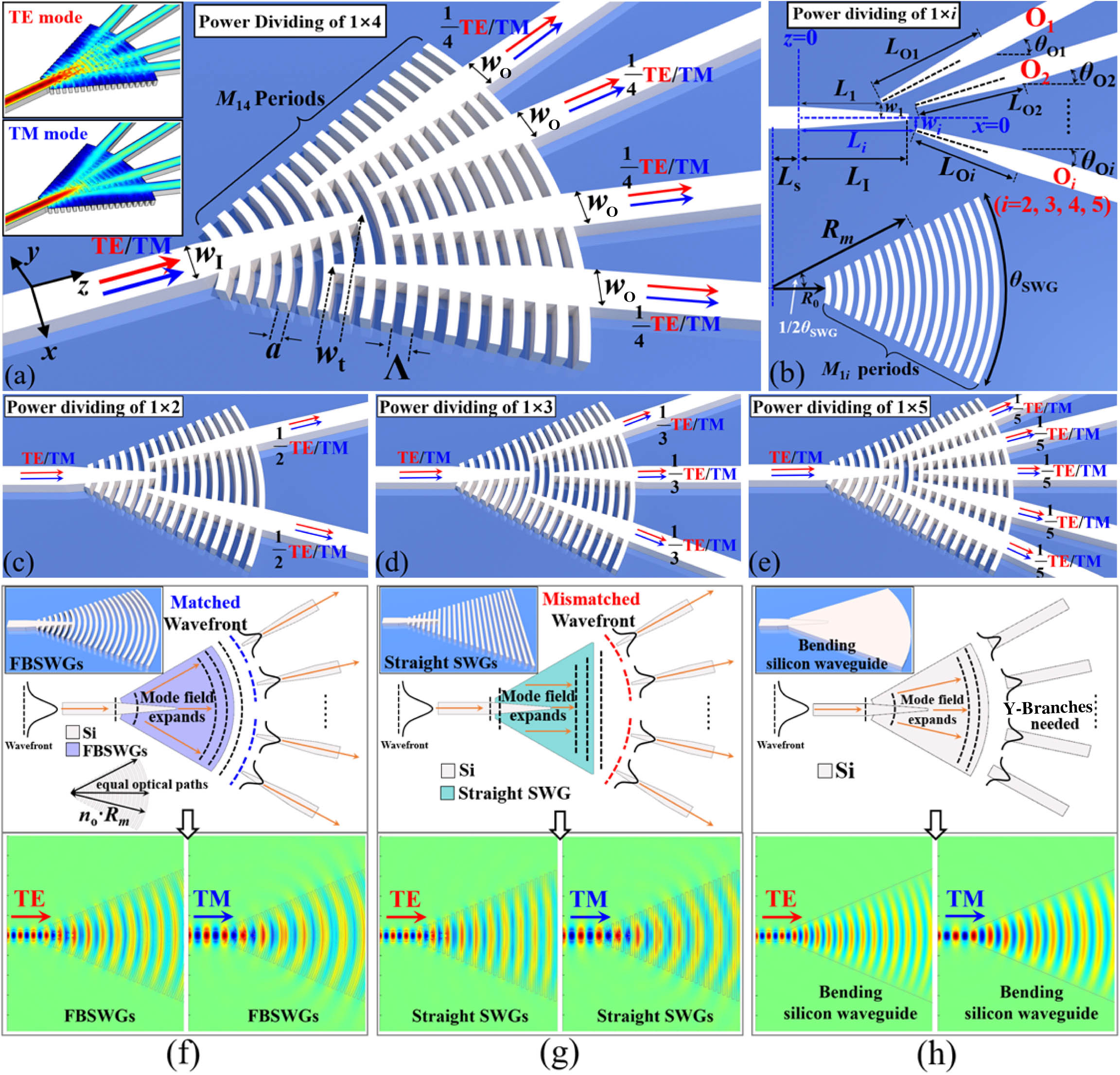
A. Configuration and Design
Figure 1 shows the schematic layouts of the proposed power splitting model for the TE/TM dual-polarization with enlarged views of simulated light propagations of the power splitting in Fig. 1(a). The , , , and power splitters are designed on the SOI platform with a 220-nm silicon core (), a 2-µm buffer oxide layer (), and a 2.2-µm silicon oxide up claddings. Here, a power splitter is composed of three sections along the direction as well as the light wave propagating direction: an input taper connected to the input waveguide, the FBSWGs forming a circular sector of degrees, and -output-angled/inverse tapers connected to output channels (namely, for the th output taper) as shown in Fig. 1(b). Specifically, the power splitter model is symmetric related to the central axis of and, here, we separate the FBSWGs from input and output tapers in Fig. 1(b) for ease of viewing. For input and output taper sections embedded in the FBSWG region, respectively, they are tapered down from to and tapered up from to in lengths of and with in the range of 1 to in which , , and denote the angle between the taper and the axis of , the crosswise position of taper in the direction, the lengthwise position of taper in the direction, respectively. As to the FBSWG region with bending angle , it is placed at the central axis of and symmetric related to it, and, meanwhile, the lengthwise position of FBSWGs in the direction is denoted by . The inner bending radius for the bending SWGs is defined as where is the inner bending radius for the th bending silicon grating wire and is the pitch for the SWG metamaterial and, thus, dimensions for the FBSWGs can be formally determined by combining , , (the period number of the FBSWGs), and . The SWG metamaterial can be considered as an equivalent homogenous medium and the effective refractive indices for SWG metamaterial waveguides () can be approximately given by Rytov’s formulas [26–28], where is the duty cycle of gratings (one has in this paper) and is the ordinary/extraordinary refractive index for polarization parallel/perpendicular to the segmenting silicon wires. In the present case, the effective refractive index of the FBSWGs should be for both TE and TM polarizations since wave vectors of expanded modes are perpendicular to the tangent direction, and, meanwhile, both TE and TM polarizations are parallel to the tangent plane of bending silicon segments of the FBSWGs. In a classical focusing grating coupler (FGC) producing curved cylindrically wavefronts, curved grating lines follow the equation (in a polar system) [36–38], where is the wavenumber in free space, is the upper-cladding refractive index, is the angle between the fiber and the chip surface normal, denotes the angle subtended by an arbitrary point on the curved grating line and to the direction, and is an integer for the th curved grating line. This equation essentially indicates that the light launched from the fiber and the light within the grating go through an equal light path or a difference of , and thereby wavefronts (or say phase fronts) are equal along the curved grating line to focus the light [39]. For the FBSWGs in this paper, the light path from the center point to the arbitrary point of the th bending grating line is and, thus, wavefronts are equal along the curved grating line for both TE and TM modes in the FBSWGs. In this way, wavefronts of light expanded/unfolded in the FBSWGs are curved correspondingly.
Sign up for Photonics Research TOC. Get the latest issue of Photonics Research delivered right to you!Sign up now
Figure 1.A 3D schematic of the proposed power splitting scheme: (a) the power splitter with enlarged views of light propagation profiles for TE and TM modes, respectively; (b) the top view of the input taper, angled output tapers, and FBSWGs, which are shown separately to facilitate the understanding; the designed (c) power splitter, (d) power splitter, and (e) power splitter. All devices are covered by claddings, which are not shown here for clarity. (f) Working principle of power splitters using FBSWGs, the optical path from the center point to the arbitrary point of the th bending grating line is , resulting in curved wavefronts, and such curved wavefronts are matched with that of angled output tapers. Comparisons of (g) conventional straight SWGs and (h) a bending silicon waveguide with the proposed FBSWG scheme. Distributions of electric-fields and for TE and TM modes are also simulated by the 3D-FDTD method and displayed in (f)–(h).
The power splitting mechanism in the present model is essentially expanding (or say unfolding) the light in an effective medium and then collecting/equally distributing it through output silicon waveguides. In this way, the key to realize an ultracompact and universal power splitting model is then twofold: (1) efficient light expanding, an area in an ultracompact length for fully and widely expanding the light with a low transition loss; (2) power collecting/distributing, output silicon waveguides for collecting the unfolded light and further distributing it equally. Unlike conventional power splitters, whose power splitting region is larger with increased , an ultracompact area for power splitting can be maintained for TE and TM modes in the proposed model. Figure 1(f) shows the operating principle and design rule of our power splitting model. In such a model, the input TE/TM mode is fully expanded in the FBSWG region with curved wavefronts. From Fig. 1(f), input TE and TM modes can be fully and widely expanded in a sector-shaped area, in an ultracompact length of μ, such as an FGC which shows a multifold length reduction compared to a standard straight grating coupler for expanding or focusing the light [36]. Subsequently, inverse and wide-angled tapers () with dimension parameters chosen carefully are embedded in the FBSWGs and able to collect and distribute the expanded light power into channels equally and adiabatically since the wavefronts of expanded modes and corresponding output modes are matched (marked by blue dotted curves) as shown in Fig. 1(f). Moreover, those angled tapers fit the ultracompact area of the FBSWGs mathematically. By taking advantages of the sector-shaped structure of the FBSWGs for the power expanding and angled tapers for the power collecting/distributing, total device lengths are all controlled within the range of [4.02, 4.25] µm only in this paper so that the , , , and power splitters are all realized within an ultracompact size. Therefore, increasing the output ports number from 2 to 5 will not lead to a much larger footprint compared with conventional power splitting schemes mentioned above, together with the polarization operation maintained, which breaks the limitations that power splitting lengths are significantly longer and polarization-sensitive operations are encountered as the output port number increases.
One may wonder if classical straight SWGs or a bending silicon waveguide structure can do the same thing. To answer this issue, we compare these two scenarios with FBSWGs in Figs. 1(g) and 1(h). For the straight SWGs, the input TE/TM mode is expanded in the strip SWGs region with straight wavefronts shaped by straight/segmenting silicon wires [see the straight dotted lines in Fig. 1(g)], and the input light is unfolded in the straight SWG region. However, the wavefronts of unfolded modes in the straight SWG region do not match those of angled output tapers and, thus, large transition losses will be generated. By contrast, if output tapers () parallel to the input tapers are used to satisfy the wavefront match, the length of the strip SWG region should be relatively long for a larger since a wide area for the full light power unfolding is required for parallel light power collection. As to the bending silicon waveguide shown in Fig. 1(h), the wavefront of the expanded mode field is matched with those of output modes. Nevertheless, multiple output Y-branches are then needed to collect and distribute the expanded modes, and such a design correspondingly encounters the designing problems of conventional Y-branches mentioned above.
B. Optimizations and Simulation Results
According to the above-mentioned operating principle and design rule, the taper lengths, angles, and positions of output tapers (), which dramatically affect the power collecting as well as distributing, are key parts to the realization of power splitters. In this way, key parameters of , , , and need to be optimized for determination. Here, the three-dimensional finite-difference time-domain (3D-FDTD) method is carried out for simulation and quantifying the device performance [40] where three figures of merit of insertion loss (IL), output uniformity (OU), and power splitting difference (PSD) for power splitter are defined as where is the optical power obtained at the output port of taper , is the optical power at the input port, and is the normalized transmission attained at the output port of taper . Essentially, both OU and PSD refer to output power uniformity, or say, power imbalance in some reports, and, here, we use PSD for easy calculation in the device optimization. Simulations are performed via 3D models where the grid sizes in the simulation process are chosen as , , and in the , , and coordinates, respectively, to mesh the structure. The computational window is set to be μμ on the plane, and is decided by the output tapers, including a 0.5-µm thickness of a perfectly matched layer boundary at each edge. For the sake of readability and simplification, only the power splitter is chosen to describe in detail, here, as an example where the input and output core widths are chosen as , to support the single mode and connect with the grating couplers, and the input taper, transferring input light to the FBSWGs, is tapered down from to in a length of μ. The initial guessing parameters of the output tapers and other fixed parameters are summarized as follows: , , μ, μ, μ, μ, μ, μ, , μ, , , , and μ. The following is the related optimization flow per run. Angles of and are swept simultaneously, and then the results (PSDs) are recorded as contour maps. To achieve low PSDs for both TE and TM modes, a trade-off is required to perform since the minimum values of PSDs for and are normally different. If the is lower than that of the last run, the and are updated and then fixed in this run with parameter ranges adjusted/narrowed for the next run. Otherwise, and remain unchanged. Next, go to Step II. (The initial guessing ranges are chosen to be [] for and [] for , respectively.)Widths of and , denoting the lateral (crosswise) position of output tapers, are swept simultaneously with fixed , and then corresponding results are recorded as contour maps. Here, a trade-off is also performed to achieve low PSDs for two polarizations. After parameter sweeps and the further trade-off process, and are updated and then fixed in this run if the new is lower than of Step I with parameter ranges adjusted/narrowed for the next run. Otherwise, and remain unchanged. Next, go to Step III. (The initial guessing ranges are chosen to be [0.2, 0.4] µm for and [0.2, 0.4] µm for , respectively.)Lengths of and , denoting the longitudinal (lengthwise) position of output tapers, are swept simultaneously with fixed and , and then corresponding results are recorded as contour maps and chosen by making a trade-off. After that, if the new is lower than of Step II, and are updated and then fixed in this run, and parameter ranges are adjusted/narrowed for the next run. Otherwise, and remain unchanged. Next, go to Step IV. (The initial guessing ranges are set to be [0.7, 1.2] µm for and [1.8, 2.4] µm for , respectively.)Lengths of output tapers and are swept simultaneously with fixed , , and , whose results are recorded as contour maps. Likewise, if the is lower than of Step III, and are updated and then fixed in this run with parameter ranges adjusted/narrowed for the next run. Otherwise, and remain unchanged. Next, go to Step V. (The initial guessing ranges are set to be [1.5, 2.5] µm for and [1.5, 2] µm for , respectively.)If the value of is higher than or equal to that of the last run, stop the optimization. Otherwise, go back to Step I and start the next run.
For each step, the feature size check is performed, which ensures the device has a minimum feature size of 100 nm for easy fabrication. Figures 2(a)–2(h) show the penultimate run of the device optimization, and no lower for both TE and TM modes can be found in the next run.
Figure 2.Calculated PSDs, respectively, for (a) the TE mode and (b) TM mode as and vary in Step I, for (c) the TE mode and (d) TM mode as and vary in Step II, for (e) the TE mode and (f) TM mode as and vary in Step III, and for (g) the TE mode and (h) TM mode as and vary in Step IV.
From Figs. 2(a) and 2(b), it is apparent that optimal/minimum and are located at two different groups of and in Step I, that is, 0.00015 for in and 0.00092 for in , respectively. In order to ensure the polarization-intensive operation of the proposed power splitter, a trade-off is performed here by choosing , where and , respectively. One sees that and , respectively, exhibit minor variations in Figs. 2(d) and 2(f). Thus, the minimum PSD for the other polarization can be chosen as long as the is lower than that of the previous step. In this way, μ, μ, μ, and μ are chosen. Similar to the trade-off performed in Figs. 2(a) and 2(b) of Step I, can be achieved by choosing μ and μ. It is worth noting that the power splitter keeps , for both TE and TM modes during the optimization flow, owing to the effective homogenous medium behavior of the FBSWGs metamaterials as well as efficient mode transitions between FBSWGs and tapers.
For the proposed power splitting model, the device length is determined by the whole grating length and output tapers simultaneously. According to Fig. 1(b), the power splitter begins at where one has for the coordinate of the FBSWG end and for the coordinate of output tapers end in the direction. Therefore, the total device length can be given by μand detailed optimal parameters of the , , and power splitters are given by Table 1 for ease of reading.
Optimized Parameters of the , , , and Power Splittersa
OPS
17
33
1.3
1.3
0.25
0.25
8
8
2.4
2.4
0.98
19
48
1.69
2.25
1.69
0.4
0
0.4
15.75
0
15.75
2.2
1.95
2.2
0.76
18
56
1.048
2
2
1.048
0.244
0.281
0.281
0.244
25
9.5
9.5
25
2
1.8
1.8
2
0.76
19
56
1.05
1.923
2.25
1.923
1.05
0.246
0.193
0
0.193
0.246
24.5
16.5
0
16.5
25.5
2
1.95
2
1.95
2
0.76
SPCb
0.5
0.5
0.1
0.6
1.82
0.12
0.22
L and w, in μm; , in degrees.
Structural parameters in common.
To verify the power dividing function of the proposed power splitter and graphically demonstrate the transmission feature, the light propagation profiles of the , , , and power splitters, operating at the central wavelength of 1.55 µm, are calculated by performing the 3D-FDTD method as shown in Figs. 3(a)–3(h). From these simulated profiles, one can clearly see that the input TE/TM mode is expanded/unfolded via a mode transition from the input waveguide to the FBSWGs where the wavefronts of the expanded modes are bent in the fan-out-curved grating lines. Meanwhile, these unfolded modes are collected by the well-designed output tapers and then equally distributed into corresponding output channels for both TE- and TM-polarized lights. Especially, the total length of the power dividing does not become larger as output splitting channels are increased in which the device lengths of , , , and power splitters lower than 4.3 µm are realized with polarization-independent operations, showing great scalability of the present power splitting model.
Figure 3.Calculated light propagation profiles as the fundamental TE/TM mode is injected for the (a) and (b) power splitter, (c) and (d) power splitter, (e) and (f) power splitter, and (g) and (h) power splitter, respectively.
The fabrication tolerances of proposed power splitters are also investigated. One can find that the designed , , and power splitters still work well even when there are some deviations of as shown in Figs. 4(a)–4(c). The 3D-FDTD method is also carried out to calculate the wavelength dependence for the optimal power splitter. Figures 4(d)–4(f) show the calculated spectral responses of the , , and power splitters over a wavelength band ranging from 1450 to 1650 nm. As is observed, the operating bandwidth is degraded as the output port number increases under the same required IL and OU level. If and are required for both TE- and TM-polarized modes, the , , and power splitters, respectively, exhibit broad bandwidths of 180 nm (1.47–1.64 µm), 190 nm (1.45–1.64 µm), and 80 nm (1.51–1.59 µm) for the polarization-independent operations.
Figure 4.Calculated ILs and OUs for the (a) power splitter, (b) power splitter, and (c) power splitter with a deviated duty cycle for both TE and TM modes. The calculated wavelength dependence of the ILs and OUs for the (d) power splitter, (e) power splitter, and (f) power splitter for TE and TM polarizations.
Furthermore, the intermodal cross talk of the proposed power splitting model is extremely low, which can be neglected. The input TE0/TM0 mode is adiabatically expanded in the FBSWGs and transited to output tapers, and only the wavefronts are shaped [see Fig. 1(f)] where higher-order modes are not excited. Besides, the width of output waveguides is set to be 500 nm for single-mode operation in which and modes are well guided, whereas, the mode is poorly supported (, rather close to the index of silica claddings), and the mode is cut off (). In this way, the higher-order modes are inherently filtered. Taking the splitter, here, as an example, we use the mode expansion method [41] to calculate the normalized transmissions of the () modes in the output ports, which are (), (), (), and (), respectively, and, thus, there are almost no higher-order modes existing in the output waveguides of the present splitter. By contrast, the normalized transmissions of the () mode in the corresponding output ports are 0.2332 (0.2401), 0.2301 (0.24007), 0.22966 (0.240082), and 0.233 (0.24009), respectively. Thus, the intermodal cross talk of proposed power splitters is extremely low and can be neglected.
3. FABRICATION AND CHARACTERIZATION
To corroborate the proposed theoretical model and corresponding simulation results, the , , and power splitters are fabricated on an SOI platform with a 220-nm-thick silicon device layer and a 2-µm buried oxide layer using 100-keV electron-beam lithography (EBL) and reactive ion etching (RIE) processes. The device patterns are defined into a material that is sensitive to electron beam exposure utilizing EBL, and then an anisotropic inductively coupled plasma RIE etching process is performed on the substrate for transferring the patterns into the underlying silicon device layer. A 2.2-µm upper-cladding layer is, subsequently, deposited using chemical vapor deposition.
Here, three-stage cascaded measure schemes are used to accurately characterize the proposed polarization-independent power splitters, together with reference waveguides composed of straight and bending nanowires. Figures 5(a)–5(h) show the microscopy images of fabricated three-stage cascaded , , and power splitters and corresponding SEM images of element power splitters. Considering the polarization-independent operation, each cascaded measure scheme is divided into two measure groups, including TE- and TM-type grating couplers, respectively. Moreover, reference straight and bending waveguides for both TE and TM modes are fabricated on the same chip for the comparison and normalization. In such a cascaded measure scheme, the output port is consistent with the th output channel of element power splitters in each stage for evaluating the optical power uniformity more precisely. Taking the power splitting measure scheme here as an example, the 3rd output channel (the central one) of each element power splitter in the first two stages is used for element cascading and then the 3rd output channel in the last stage (named output port ) is used for the characterization. For equal power distributions, the , , , and power splitters, respectively, have splitting factors of 3 dB, 4.77 dB, 6.02 dB, and 6.98 dB in each output channel. By using the three-stage cascaded scheme, the transmittance in each of output channels for the designed power splitter can be obtained by [42]where is the measured and normalized transmittance in the output port as shown in Figs. 5(b), 5(e), and 5(f) with ranging from 1 to .
Figure 5.(a) Microscope image of the reference TE and TM waveguides. (b) Microscope image of the three-stage cascaded measure scheme for the fabricated power splitters and (c) and (d) corresponding scanning electron microscope (SEM) images of fabricated power splitters. Microscope image of the three-stage cascaded measure scheme for the fabricated (e) power splitters and (f) power splitters. Pseudocolor SEM images of (g) the and (h) the power splitting elements.
Here, a tunable laser (Santec TSL-710) and an optical power meter (Santec MPM-210) are utilized for measuring the transmittance spectra of the fabricated , , and optical power splitters, and the characterized normalized transmittances are shown in Figs. 6(a)–6(f). From the spectra, one can observe that the fabricated power splitters have good uniformity for polarization-independent equal light power distributions where the normalized transmittances for both TE and TM modes of the , , and power splitters are around , , and , corresponding to the 33.3%, 25%, and 20% power splittings, respectively. For the fabricated optical power splitter, corresponding ILs (OUs) for TE and TM modes are measured to be 0.75 dB and 0.58 dB (0.64 dB and 0.32 dB), respectively, at the central wavelength of 1.55 µm. From Fig. 6(b), the power splitting for the TM mode has and within the wavelength range of 1500 to 1570 nm. One has a working bandwidth as large as 54 nm (1513–1567 nm) for achieving an for both TE- and TM-polarized lights. Regarding the fabricated power splitter, the measured IL and OU are 1.16 dB/0.66 dB and 0.8 dB/0.43 dB for the input TE/TM mode at 1550 nm, respectively, and ILs and OUs are lower than 1.35 dB and 1 dB over a 49-nm bandwidth (1512–1561 nm) for both TE and TM modes. As to the fabricated power splitter, the performance is degraded as the number of output channels is increased. The measured IL/OU of TE mode power splitting is 1.24 dB/0.65 dB and the IL/OU of TM mode power splitting is 0.73 dB/0.54 dB at 1550 nm, respectively. For both TE and TM modes, the measured ILs and OUs are lower than 1.65 dB and 1 dB, respectively, over an operating bandwidth of 38 nm (1521–1559 nm). One can clearly find that the performance of TE modes has larger fluctuations than that of TM modes across the operation bandwidth, which is mainly due to the higher sensitivity to sidewall roughness of the TE mode in the FBSWG metamaterials as well as input/output grating couplers. Furthermore, the large fluctuations at long wavelength () are caused by the blueshifted central wavelength of the fabricated grating couplers.
Figure 6.Measured and normalized transmittance spectra of the power splitter for the input (a) TE and (b) TM modes, the power splitter for the input (c) TE and (d) TM modes, and the power splitter for the input (e) TE and (f) TM modes, respectively.
Table 2 gives a brief comparison with previous reported power splitters. One can observe that the proposed and power splitters have the shortest device lengths and competitive ILs as well as OUs. More importantly, our power splitting model can maintain an ultracompact length of μ and a polarization-independent operation as the number of output channels increases from 2 to 5, whereas other power splitters can only realize a specific power splitter even with polarization-dependent operations [11,17,20,22].
Comparison of Several Power Splitters at the Wavelength of 1.55 μm
Structure
Function
Length (µm)
IL (dB)
OU (dB)
Bandwidth (nm)c
Sima
Expb
Sim
Exp
Sim
Exp
Y-branch [11]
at TE
4000
0.26
–
100 ()
100 (, )
at TM
–
100 ()
100 (, )
Tapers [17]
at TE
12.5
0.18
–
100 ()
40 (, )
MMI [20]
at TE
36
0.42
0.61
150 (, )
104 (, )
DCs [22]
at TE
7.3
0.016
0.068
0.058
111 (, )
50 (, )
at TM
0.065
0.62
0.021
90 (, )
54 (, )
This work
at TE
4.24
0.43
0.75
0.023
0.64
180 (, )
54 (, )
at TM
0.24
0.58
0.015
0.32
at TE
4.02
0.33
1.16
0.066
0.8
190 (, )
49 (, )
at TM
0.18
0.66
0.0005
0.43
Simulated results.
Experimental results.
IL and OU shown in parentheses are in dB.
4. CONCLUSION
In conclusion, we have proposed an ultracompact, polarization-independent, and scalable power splitting model by using the FBSWG metamaterials instead of straight SWGs. For both input TE and TM modes, they can be effectively expanded by the FBSWGs within an ultracompact region. Due to the same optical path from the input taper to the bending grating lines, wavefronts of expanded TE and TM modes are curved. By using -angled output tapers with optimized parameters to match these wavefronts, the TE and TM modes expanded by the FBSWGs can be collected and evenly distributed into -output channels through that ultracompact region. Based on such a splitting model, a , a , a , and a OPSs are designed, and the latter three are experimentally demonstrated with device lengths all lower than 4.3 µm, which are the shortest , , and OPSs with polarization-independent operations reported until now, to our knowledge. The measurements show low ILs (, , and ) and low OUs (, , and ) over bandwidths of 54 nm (1513–1567 nm), 49 nm (1512–1561 nm), and 38 nm (1521–1559 nm) for the , , and power splitters, respectively. Different from conventional power splitters, the proposed model is the first power splitting configuration in which an ultracompact device length (μ) and a polarization-independent operation can be maintained simultaneously when the output channels are increased from 2 to 5 as far as we know. We believe such a power splitting model could find its applications in ultra-high-density on-chip PICs and further provide new insight into the development of ultracompact, scalable, and polarization-independent integrated nanophotonic devices.