Wenjing Xu, Jie Chen, Zhangqu Kuang, Li Zhou, Ming Chen, Chengbin Zhang. A low-power high-quality CMOS image sensor using 1.5 V 4T pinned photodiode and dual-CDS column-parallel single-slope ADC[J]. Journal of Semiconductors, 2022, 43(8): 082401
Copy Citation Text
This paper presents a low-power high-quality CMOS image sensor (CIS) using 1.5 V 4T pinned photodiode (4T-PPD) and dual correlated double sampling (dual-CDS) column-parallel single-slope ADC. A five-finger shaped pixel layer is proposed to solve image lag caused by low-voltage 4T-PPD. Dual-CDS is used to reduce random noise and the nonuniformity between columns. Dual-mode counting method is proposed to improve circuit robustness. A prototype sensor was fabricated using a 0.11 µm CMOS process. Measurement results show that the lag of the five-finger shaped pixel is reduced by 80% compared with the conventional rectangular pixel, the chip power consumption is only 36 mW, the dynamic range is 67.3 dB, the random noise is only 1.55 e–rms, and the figure-of-merit is only 1.98 e–·nJ, thus realizing low-power and high-quality imaging.This paper presents a low-power high-quality CMOS image sensor (CIS) using 1.5 V 4T pinned photodiode (4T-PPD) and dual correlated double sampling (dual-CDS) column-parallel single-slope ADC. A five-finger shaped pixel layer is proposed to solve image lag caused by low-voltage 4T-PPD. Dual-CDS is used to reduce random noise and the nonuniformity between columns. Dual-mode counting method is proposed to improve circuit robustness. A prototype sensor was fabricated using a 0.11 µm CMOS process. Measurement results show that the lag of the five-finger shaped pixel is reduced by 80% compared with the conventional rectangular pixel, the chip power consumption is only 36 mW, the dynamic range is 67.3 dB, the random noise is only 1.55 e–rms, and the figure-of-merit is only 1.98 e–·nJ, thus realizing low-power and high-quality imaging.
1. Introduction
CMOS image sensors (CISs) have been widely used in many application fields such as mobile phones and wearable devices. In recent years, the application of CIS has gradually expanded to the internet of things (IoT) and artificial intelligence (AI) fields. On the one hand, IoT and AI devices only have small batteries for energy support, yet they are expected to last weeks on a single charge. On the other hand, CIS serves as the eyes of the machine to see the world, which leads an increasing demand for high-quality imaging. Therefore, it is crucial to design both low-power and high-performance CISs[1, 2].
The basic idea to reduce power consumption is to lower the supply voltage. The supply voltage of the CIS readout circuit is limited by the voltage of the pixels. Digital pixels are usually used to reduce the pixel voltage. In 2010 JSSC[3], a digital pixel that works under 0.5 V was proposed but its dynamic range was only 21.3 dB. Later in 2015 JSSC[4] and 2021 JSSC[2], although the dynamic range has been increased to 42 and 52 dB, respectively, there was still a gap compared with high-quality imaging.
High-quality imaging usually requires the use of active pixels. 1.5 V 3T pixel has been proposed in 2003 TED[5]. But compared with 4T pixel, 3T pixel cannot achieve true correlated double sampling, and thus the random noise is larger. The 4T pinned photodiode (4T-PPD) active pixel is the most commonly used pixel structure for high-performance CIS. Traditionally, the supply voltage of 4T-PPD is greater than 2.8 V. When the voltage drops, the electrons far away from the transfer gate lack lateral electric field and stay in the pixel, causing image lag. In 2016 JSSC[6], 4T-PPD active pixel was designed to work at 0.9 V by improving the pixel timing; however, the random noise was as high as 83 e–rms, and the dynamic range was only 50 dB.
Therefore, how to realize low-voltage 4T-PPD while maintaining high image quality is a critical issue. In this work, a low-power high-quality CIS using 1.5 V 4T-PPD and dual correlated double sampling (dual-CDS) column-parallel single-slope ADC (SS-ADC) is proposed. A five-finger shaped pixel layer instead of traditional rectangular shape is used to solve image lag caused by low-voltage 4T-PPD. Dual-CDS is used to reduce the random noise and the nonuniformity between columns. The dual-mode counting method is used to improve the circuit's robustness.
2. Overall architecture
Among several types of column-parallel ADCs, SS-ADC[7-10] is clearly the most widely used because a SS-ADC can be implemented using a very simple column circuit, which mainly consists of a single comparator and a counter. Moreover, this simple column circuit also makes it relatively easy to ensure uniformity between columns, and thus minimizes the readout noise.
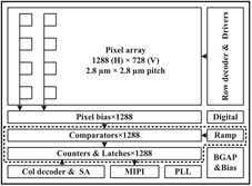
Fig. 1 shows the architecture of the proposed CIS. The pixel array is 1288 × 728 and the pixel pitch is 2.8 μm. The Row-decoder sequentially selects a single row line for signal readout processing. The signal charges generated at the PPD are converted to the signal voltage on the vertical signal lines. The comparator array compares the readout signals with the ramp generator output. The comparator changes at the timing when the ramp voltage reaches the signal voltages. Then, the counter stops counting and the latch array latches the counter outputs. The Col-decoder sequentially selects latched ADC value, and the sense amplifier (SA) outputs 10 b straight binary data to MIPI interface. PLL provides high-speed clock for digital control circuit and MIPI circuit.
Figure 1.Block diagram of the overall architecture.
A typical 4T-PPD active pixel[10] is shown in Fig. 2. The 4T-PPD consists of the PPD, transfer gate (TG), floating diffusion (FD) and three transistors. A PPD is a device made by a n- well buried in a p- substrate, and a thin p+ layer covers the n- well. The pinned photodiode has no contacts, and the photogenerated electrons are transferred to the FD node by the operation of the TG. Due to physic limitations of the PPD and the TG structure, transferring all of the electrons completely from the photodiode is very hard, especially for low-voltage PPD.
The dotted line in Fig. 2 is the charge transfer path when a high voltage is applied to the VTG. Traditionally, VTG is greater than 2.8 V, so that a fringe field from the edge of the PPD (marked as A) to TG (marked as C) is formed, pushing the electrons to TG completely. When VTG drops, due to the absence of the fringe field, the electrons moving from A to B mainly rely on thermal diffusion and self-induced drift, which takes a long time. Finally, the electrons are left behind in the PPD, and these remaining electrons create image lag.
To reduce the image lag caused by low-voltage PPD, 2.8 µm small pixel pitch is used to reduce the electron diffusion distance. To further accelerate the movement of photogenerated charges without changing the process steps and conditions, the shape of the PPD layer might be changed to create an electric field from the edge of PPD to TG. In previous studies[11-15], triangle, W-shape, trapezoid, and L-shape PPD have been reportedly, but all these designs aim at large-sized pixels. For small-sized pixels, the PPD layer should not be cut too much; otherwise, it would affect the full-well capacity and reduce the dynamic range.
Therefore, for the small pixel design in this paper, the traditional rectangular PPD layer shown in Fig. 3(a) is improved into a five-finger PPD layer, which can be seen in Fig. 3(b). The number five is the result of a balance between full-well capacity and the transfer speed. If the number of fingers is too small, then too much of the photosensitive area will be cut, which will greatly reduce the full well capacity. In contrast, if the number of fingers is too large, then the inclination angle of each finger will not be enough, which will decrease the charge transfer speed. The cutting method is as follows. First, the center of the TG is marked as point C, the black rectangular frame is the farthest area from point C, and thus the area is cut out. Then, the four arrow lines divide 90° into five equal parts, and the length of each arrow line is basically the same. This design is developed to ensure that the time for the photo-generated charges in each area to move to the TG is nearly the same. The angles of the five fingers are almost 110°, based on the experiment results reported in Ref. [12]. The area of the PPD layer that is finally cut off accounts for 14% of the total rectangular area of 4.27 µm2.
Compared with the conventional rectangle shaped PPD shown in Fig. 3(a), the width of the photodiode becomes narrower the farther away from transfer gate. The five-finger shaped PPD utilizes the narrow width effect to create the extra electrical field in the direction of the charge transfer. This causes more electrons to be pulled out of the PPD. The potential profile of a rectangular PPD is shown in Fig. 3(a). There is no potential gradient forcing electrons because there is no narrow channel effect. A potential gradient is formed in the five-finger shaped PPD as shown in Fig. 3(b). The proposed five-finger shaped PPD can not only accelerate the electrons transfer from PPD to TG but can also meet the requirements of full-well capacity and dynamic range due to the small cropped area.
4. Design of the column-parallel SS-ADC
The column circuit of the SS-ADC is shown in Fig. 4. To further reduce power consumption, the comparator is implemented by a two-stage comparator. The pixel output signal Vpixel and ramp signal Vramp are, respectively, connected to the negative and positive input terminals of the first-stage comparator through capacitors C1A and C1B. In this way, both Vpixel and Vramp are ac-coupled, thus voltages of Vpixel and Vramp are not limited by the first-stage input common mode voltage. Moreover, a fully differential first stage can avoid systematic offset. A capacitor C2 is added between the first-stage and the second-stage to eliminate the offset of the first-stage. The output signal of comparator Com_out becomes Com_new after passing the DDS_MODE module. The column counter, composed of ripple counter, performs the A/D conversion by counting the number of clocks until the comparator output changes. A ripple counter has the advantage of not needing to be synchronized with the high-speed clock.
To reduce random noise and the nonuniformity between columns, dual-CDS which includes analog correlated double sampling and digital double sampling is used. Fig. 5 shows the timing diagram for the dual-CDS operation.
Figure 5.Timing diagram for dual correlated double sampling.
The dual-CDS operation is as follows. 1) Switches S1 and S2 are turned on, the comparator is reset. When the control signal VRST is high, the pixel reset level Vprst appears at the pixel output. Then S1 and S2 are turned off. Non-overlap S1 and S2 are designed to reduce non-idealities introduced by clock feedthrough and charge injection. At this time, the voltages of the negative and positive input terminals of the comparator can be expressed as
whereVcm is the common-mode voltage of the comparator, and Vos is the comparator offset. 2) Then, Vramp starts to change near Vramp0, the positive input terminal of the comparator can be expressed as
The difference between the two ends of the comparator is derived by Eq. (3) minus Eq. (1) as
When ∆Vcom1> 0, the comparator flips, the ripple counter stops counting, and the count value is num1. 3) When the control signalVTG is high, the pixel signal level Vpsig appears at the pixel output. And the negative input terminal of the comparator can be expressed as
The difference between the two ends of the comparator is derived by Eq. (3) minus Eq. (5) as
When ∆Vcom2> 0, the comparator flips, the ripple counter stops counting, and the count value is num2. The final 10-bit counting number Dout is given as
Analog CDS is used to eliminate the offset of the pixel. The offset of the comparator and counter variations that cause A/D conversion error are corrected by digital CDS. Due to the use of the digital CDS method, the conversion time is increased by 20% because of the time for num1 counting. To achieve 30 fps at 1288 × 728, the clock frequency of the ripple counter is 72 MHz. After dual-CDS subtraction, the system non-idealities are well canceled.
4.2. Dual-mode counting method
The total number of counts directly relates to the difference between the pixel reset level and signal level. In extreme cases, when the scene is complete bright, all column-parallel counters start counting at the same time and do not stop until they are all full. On one hand, this introduces a lot of spikes in the substrate, resulting in supply noises. On the other hand, the high-power current flows from the ADC supply may pull down the supply level significantly due to parasitic resistance of the chip and package, which causes the chip to fail.
To solve the problem, a dual-mode counting method is proposed (i.e., even-column and odd-column counters start and stop counting at different times). As shown in Fig. 4, the output of the comparator connects to the counter through the DDS_MODE module, and the circuit of the DDS_MODE module is shown in Fig. 6(a). The proposed counting algorithm is illustrated in Fig. 6(b). When DDS_MODE = 1, Com_new is the same as Com_out, and the final Dout expression of even columns is the same as Eq. (8). When DDS_MODE = 0, Com_new is the opposite of Com_out, the odd columns start counting when the even columns stop, and stop counting when the Vramp stops changing. The final Dout expression of the odd columns is given as
With this counting method, whether the scene is complete dark or bright, the digital power supply level and ground level variation are almost the same, and thus circuit robustness is improved.
5. Measurement results
A prototype sensor was fabricated using a 0.11 µm 1P3M CMOS process. Fig. 7 shows a photograph and layout of the chip. The size of the whole chip is 4.8 mm (H) × 2.9 mm (V). The pixel array is 1288 × 728 and the pixel pitch is 2.8 μm.
The test pixel in chip3 is rectangle shaped, as shown in Fig. 3(a), while the test pixel in chip4 is five-finger shaped as shown in Fig. 3(b). The doping profiles of chip3 and chip4 are the same. Fig. 8 compares the measured lag performance of two different pixel designs. It can be seen that the lag of the rectangle shaped pixel gradually increases with the increase of light intensity, while the lag of the improved five-finger shaped pixel almost does not change. At the maximum exposure, the lag of the five-finger shaped pixel is reduced by 80% compared with the conventional rectangle shaped pixel.
Figure 8.(a) Timing diagram for lag test. (b) Measured lag curves with different shaped PPD.
In the high-light region, the full-well capacity of the five-finger PPD decreases from 647 mV (5119 e−) to 623 mV (4928 e−) compared with the rectangle shaped pixel because the area of the PPD layer is reduced by 14%. However, CIS only works in the linear region of the photoelectric response curve, so a slight decrease in the full-well capacity will not affect the CIS. The dark current values for five-finger and rectangle shaped pixels are 5.01 and 5.06 mV/s respectively.
Fig. 9 shows the measured photo response curves of five-finger shaped PPD with different transfer gate voltage. The photo response curves are nearly the same by changing VTG. This is because the five-finger shaped pixel improves the electrons transfer efficiency, thus almost complete transfer can be realized (even at a low voltage of 1.5 V).
Figure 9.Measured photo response curves of five-finger shaped PPD with different transfer gate voltage.
Fig. 10 shows the measured photon transfer curve versus input light intensity. A dark random noise of 1.55 e–rms is achieved with a pixel conversion gain of 126.4 μV/e−. This chip achieves a dynamic range of 67.3 dB.
Figure 1.Block diagram of the overall architecture.
A sample image taken with the CIS at 1.5 V analog and 1.2 V digital supply voltage is shown in Fig. 11. Image lag due to the 1.5 V 4T-PPD is negligible at 30 fps.
To verify the validity of the dual-mode counting method, the test is carried out as follows. The entire chip is illuminated by a parallel light source, while the lower left-hand and lower right-hand corners of the photosensitive area are covered with insulating black tape. The pixel arrays covered by black tape are both 472 × 345. The measured digital codes of the 644th column with or without dual-mode counting is shown in Fig. 12. When dual-counting method is off, the quantization environments between the first 383 lines and the last 345 lines of the 644th column are inconsistent, so the code values have a minimum deviation of 2 LSB. When dual-counting method is on, the code value consistency between the first 383 lines and the last 345 lines of the column 644th is better.
Table 1 shows the measured power consumption at 30 fps. Because a low-voltage 1.5 V 4T-PPD is used, the supply voltage of the subsequent analog readout circuit can also be 1.5 V, which greatly reduces the power consumption of the whole chip. To further reduce power consumption, the supply voltage of the digital circuit is 1.2 V, and the I/O PAD supply is 1.8 V. The measured total power consumption is only 36 mW.
Table 2 shows a performance summary of the proposed CIS and a comparison with other works. To evaluate the energy efficiency of an image sensor, FoM can be calculated as follows[16]:
This work achieves a FoM of 1.98 e−·nJ. Compared with previous woks, the proposed CIS realizes low-power by using 1.5 V 4T-PPD, while maintaining high image quality.
6. Conclusion
This work presents a low-power high-quality CIS using 1.5 V 4T-PPD and column-parallel SS-ADC. A five-finger shaped pixel layer is proposed to solve image lag caused by low-voltage 4T-PPD. Dual correlated double sampling is used to reduce random noise and the nonuniformity between columns. To improve circuit robustness, dual-mode counting method is proposed. Measurement results show that the lag of the five-finger shaped pixel is reduced by 80% compared with the conventional rectangular pixel, the chip power consumption is only 36 mW, the dynamic range is 67.3 dB, the random noise is only 1.55 e–rms, and the FoM is only 1.98 e–·nJ. The proposed CIS realizes low-power by using 1.5 V 4T-PPD while maintaining high image quality, which is suitable for IoT and AI applications.
Acknowledgements
This work was supported by the National Key R&D Program of China (2019YFB2204304).
[7] Y Nitta, Y Muramatsu, K Amano et al. High-speed digital double sampling with analog CDS on column parallel ADC architecture for low-noise active pixel sensor. 2006 IEEE International Solid State Circuits Conference, 2024(2006).
[9] I Park, C Park, J Cheon et al. A 76mW 500fps VGA CMOS image sensor with time-stretched single-slope ADCs achieving 1.95e- random noise. 2019 IEEE International Solid-State Circuits Conference, 100(2019).
Wenjing Xu, Jie Chen, Zhangqu Kuang, Li Zhou, Ming Chen, Chengbin Zhang. A low-power high-quality CMOS image sensor using 1.5 V 4T pinned photodiode and dual-CDS column-parallel single-slope ADC[J]. Journal of Semiconductors, 2022, 43(8): 082401