• Journal of Semiconductors
  • Vol. 41, Issue 12, 122803 (2020)
Narendra Yadava, Shivangi Mani, and R. K. Chauhan
Author Affiliations
  • Department of Electronics & Communication Engineering, Madan Mohan Malaviya University of Technology, Gorakhpur 273010, Indian
  • show less
    DOI: 10.1088/1674-4926/41/12/122803 Cite this Article
    Narendra Yadava, Shivangi Mani, R. K. Chauhan. RF performance evaluation of p-type NiO-pocket based β-Ga2O3/black phosphorous heterostructure MOSFET[J]. Journal of Semiconductors, 2020, 41(12): 122803 Copy Citation Text show less
    (Color online) (a) P-type NiO-pocket based β-Ga2O3 MOSFET. (b) P-type NiO-pocket based β-Ga2O3/black phosphorous heterostructure MOSFET.
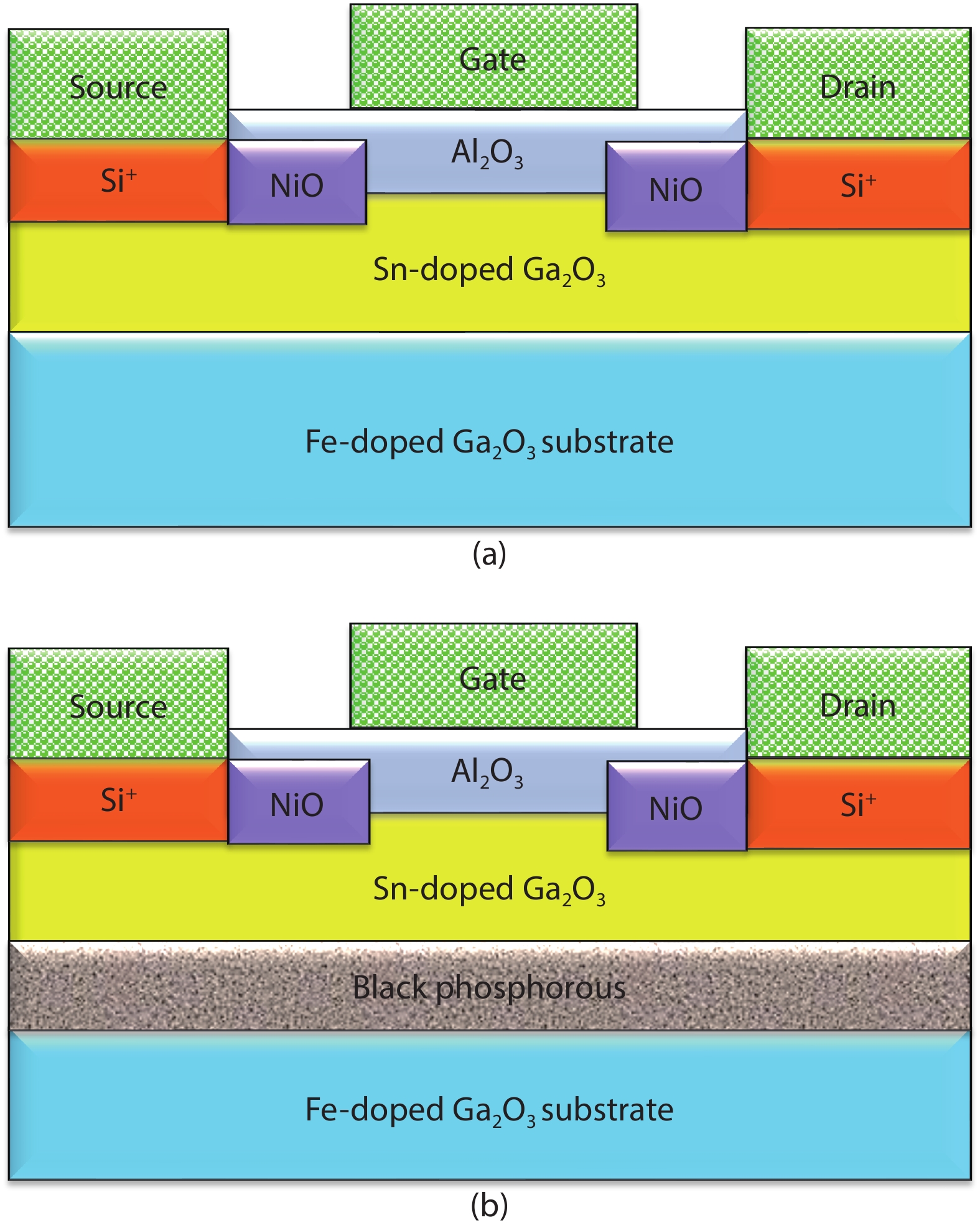
    Fig. 1. (Color online) (a) P-type NiO-pocket based β-Ga2O3 MOSFET. (b) P-type NiO-pocket based β-Ga2O3/black phosphorous heterostructure MOSFET.
    (Color online) Lattice temperature in (a) β-Ga2O3 MOSFET and (b) P-type NiO-pocket based β-Ga2O3 MOSFET.
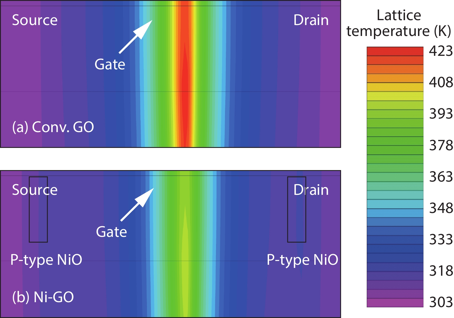
    Fig. 2. (Color online) Lattice temperature in (a) β-Ga2O3 MOSFET and (b) P-type NiO-pocket based β-Ga2O3 MOSFET.
    (Color online) Potential distribution in (a) β-Ga2O3 MOSFET and (b) P-type NiO-pocket based β-Ga2O3 MOSFET.
    Fig. 3. (Color online) Potential distribution in (a) β-Ga2O3 MOSFET and (b) P-type NiO-pocket based β-Ga2O3 MOSFET.
    (Color online) Transfer (ID–VGS) and transconductance (gm) behavior of the devices. Inset: ID–VGS in log-scale.
    Fig. 4. (Color online) Transfer (IDVGS) and transconductance (gm) behavior of the devices. Inset: IDVGS in log-scale.
    (Color online) Output characteristics (ID–VDS) of the devices.
    Fig. 5. (Color online) Output characteristics (IDVDS) of the devices.
    (Color online) Output conductance (gd) behavior of the devices.
    Fig. 6. (Color online) Output conductance (gd) behavior of the devices.
    (Color online) Intrinsic capacitance (Cgs) versus gate voltage (VGS). Inset: fT versus VGS.
    Fig. 7. (Color online) Intrinsic capacitance (Cgs) versus gate voltage (VGS). Inset: fT versus VGS.
    (Color online) Intrinsic capacitance (Cgd) versus gate voltage (VGS). Inset: GBW versus VGS.
    Fig. 8. (Color online) Intrinsic capacitance (Cgd) versus gate voltage (VGS). Inset: GBW versus VGS.
    (Color online) (a) Output power (POUT) versus input power (PIN). (b) Power-added-efficiency (PAE) versus input power (PIN). Inset: Output power gain (GP) versus PIN.
    Fig. 9. (Color online) (a) Output power (POUT) versus input power (PIN). (b) Power-added-efficiency (PAE) versus input power (PIN). Inset: Output power gain (GP) versus PIN.
    Parameterβ-Ga2O3[4]Black phosphorous[14]
    Bandgap energy (eV)4.81.88
    Local conduction band density of states (1017 cm−3) 37.20.3
    Work function (eV)5.234.56
    Electron affinity (eV)4.05.5
    Relative permittivity (F/m)10.06.1
    Table 1. Material parameters used in the simulation of the β-Ga2O3/BP heterostructure MOS device.
    ReferenceMOSFETCgs(pF) Cgd(pF) fT(GHz) GBW (GHz)POUT (dBm) (PAE) (%)GP (dB)
    Ref. [8] Exp. GO3.3013.716.35.10
    Refs. [4, 17] Conv. GO (Exp. GO. by Higashiwaki et al.) 0.330.131.870.520.645.810.50
    GO/BP0.430.221.770.6415.113.015.31
    Ref. [22] NiO-GO0.290.131.270.4819.304.89.75
    This workNiO-GO/BP0.230.181.370.5114.732.813.02
    Table 2. RF performance comparison of the reported gallium oxide MOSFETs with the proposed NiO-GO/BP MOSFET.
    Narendra Yadava, Shivangi Mani, R. K. Chauhan. RF performance evaluation of p-type NiO-pocket based β-Ga2O3/black phosphorous heterostructure MOSFET[J]. Journal of Semiconductors, 2020, 41(12): 122803
    Download Citation